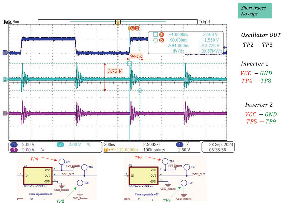
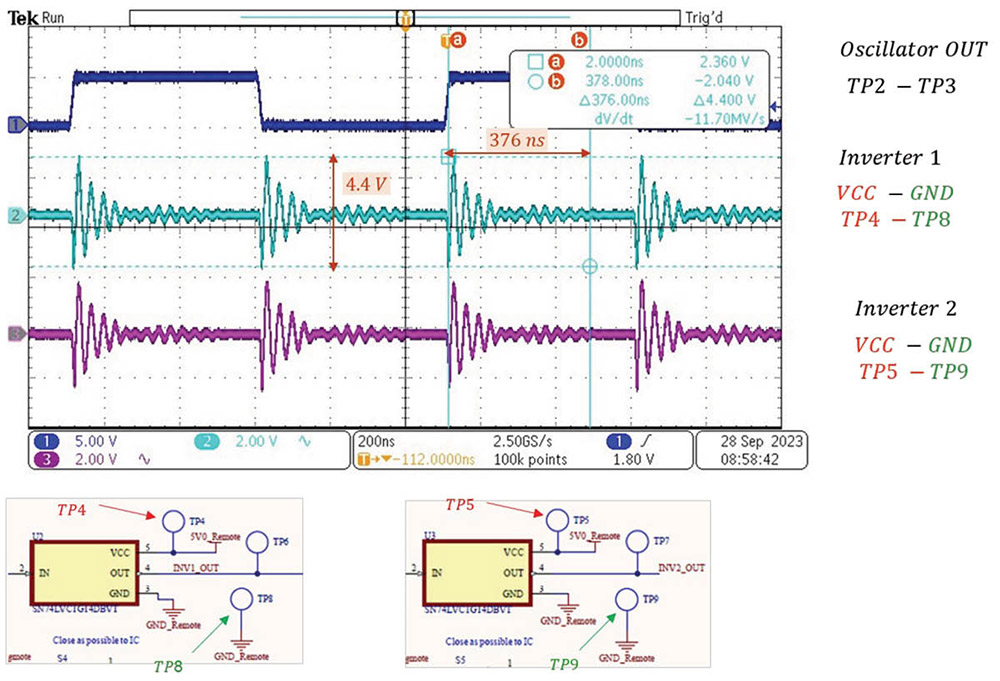
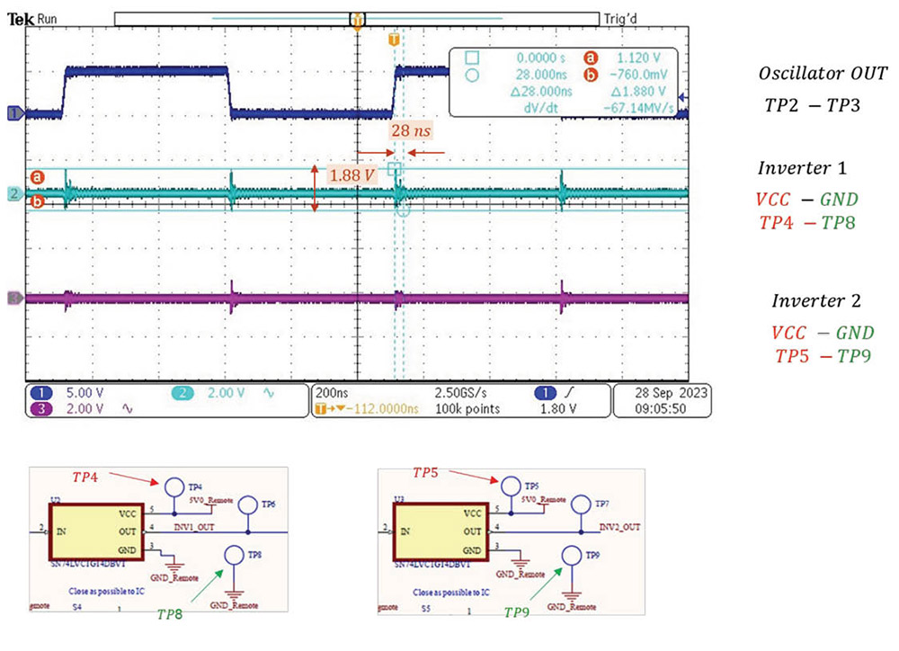
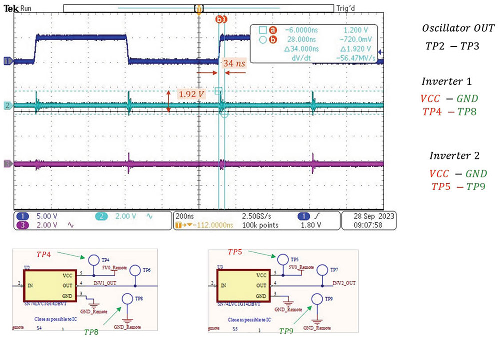
his article describes a laboratory experiment that shows the impact of the decoupling capacitors and a PCB trace length on the signal integrity in a CMOS inverter circuit.
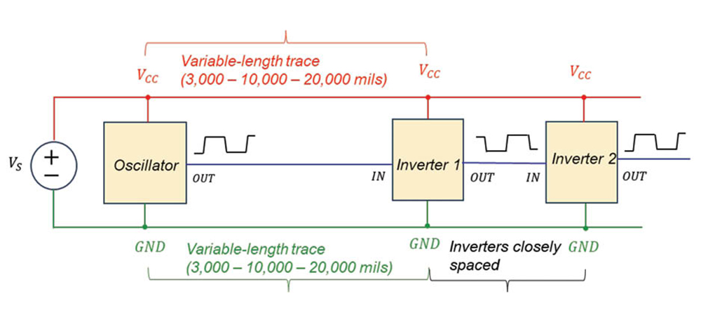
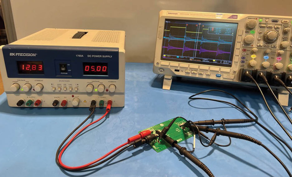
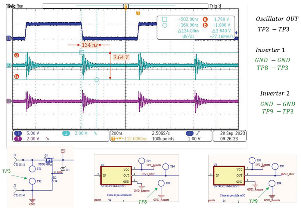
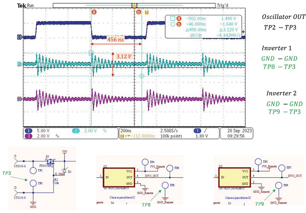
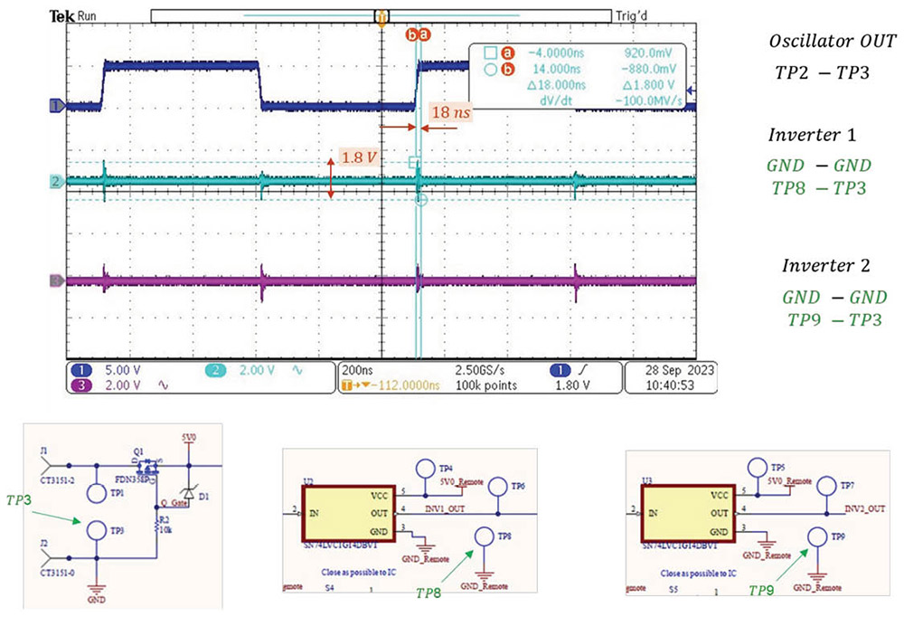
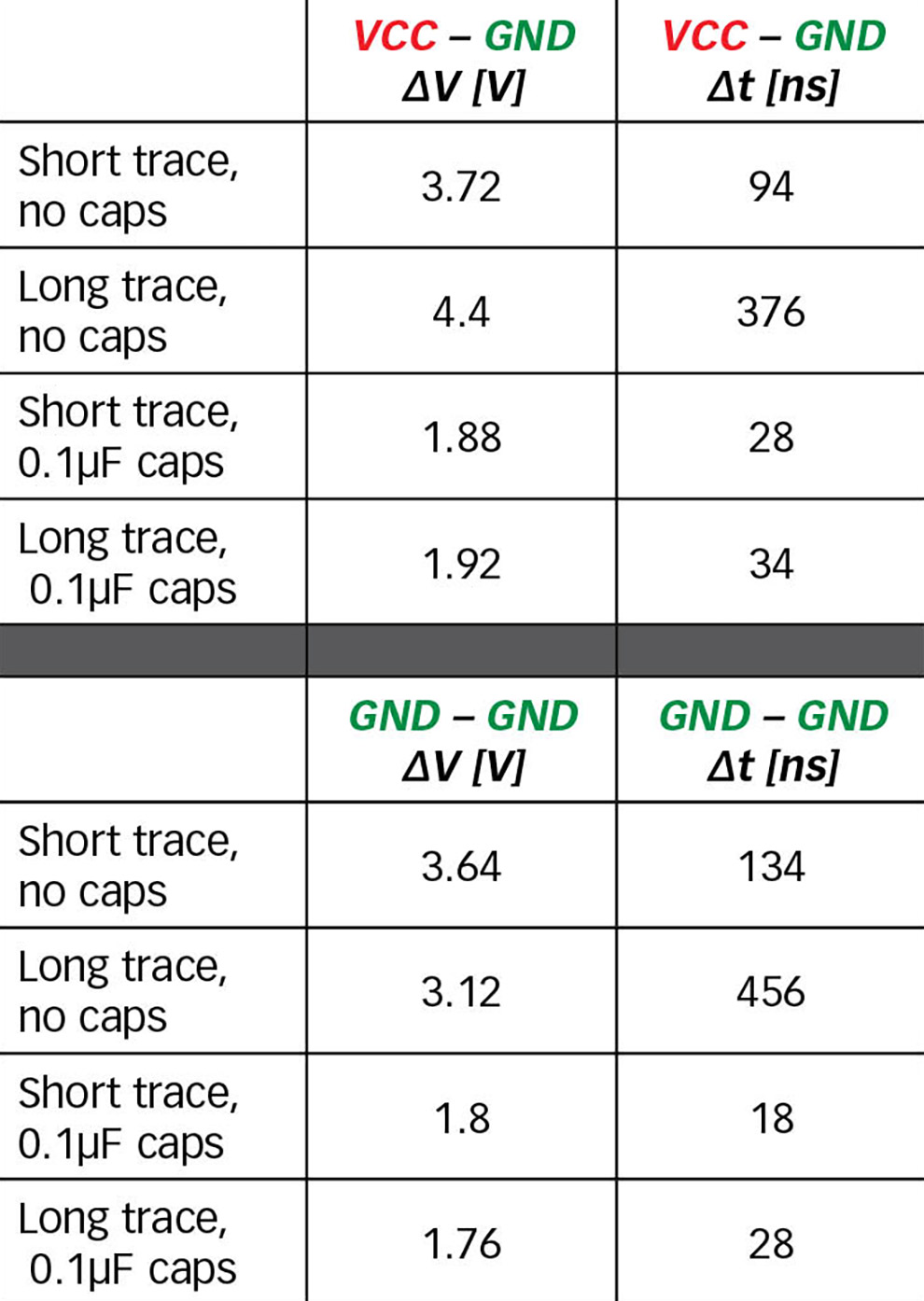
During switching, a transient current is drawn from the source. The inductance associated with the current loop causes the voltages at the power and ground pins to deviate from the desired values, as shown in the measurement section (see [1] for more details).
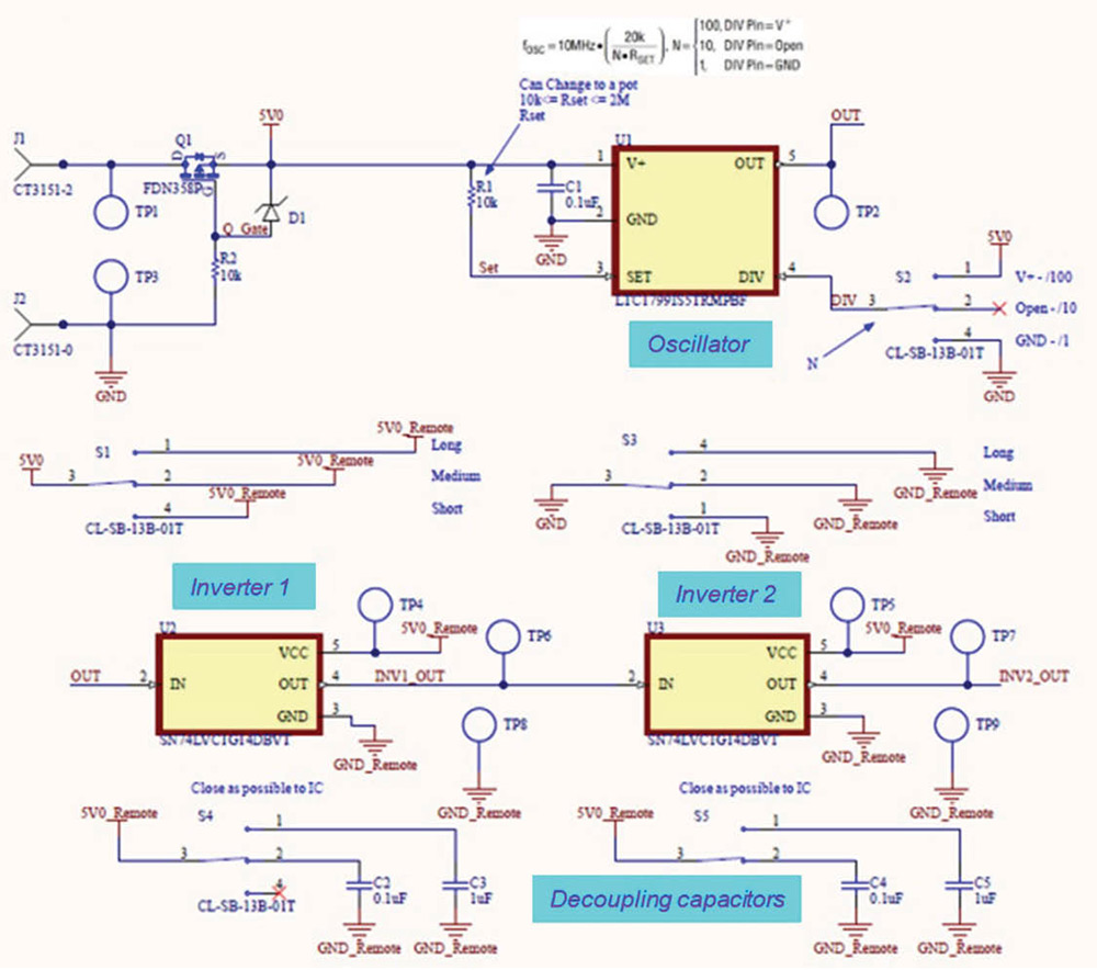
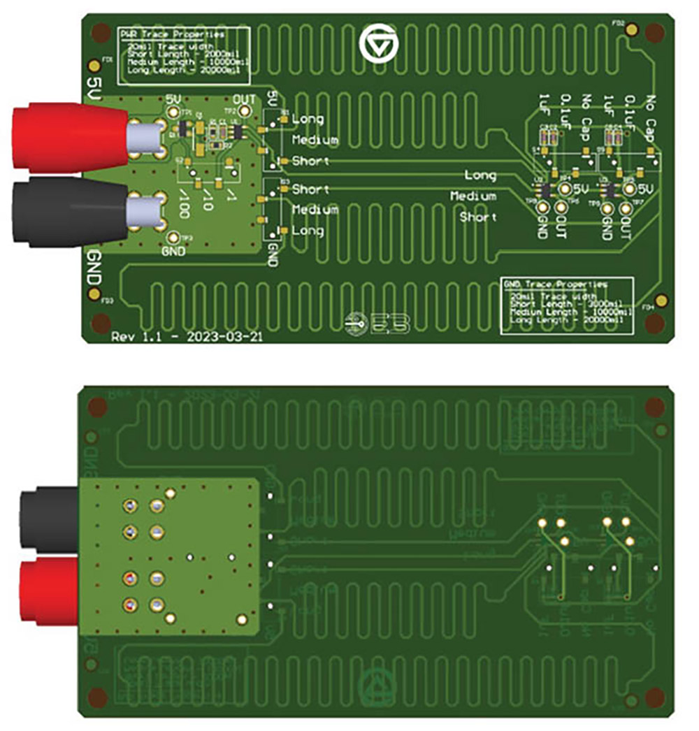
The board was purposely designed with very long traces to show the negative impact of the associated inductance while increasing the impact of a decoupling capacitor at the same time.

The upcoming March 2024 column will discuss the impact of a decoupling capacitor and trace length on radiated emissions. Measurements will be performed in a semi-anechoic chamber, in accordance with CISPR 25 Edition 5 automotive standard, a monopole antenna was used in the frequency range of 150 kHz – 30 MHz, a biconical antenna in the range of 30 MHz – 300 MHz, and a log-periodic antenna in the range of 300 MHz – 1GH.
The April 2024 column will be devoted to conducted emissions measurements in accordance with the same standard. Measurements will be performed in the same semi-anechoic chamber, both on the battery and ground lines in the frequency range of 150kHz – 108 MHz.
- Bogdan Adamczyk, “Impact of a Decoupling Capacitor in a CMOS Inverter Circuit,” In Compliance Magazine, September 2019.
- Bogdan Adamczyk, Principles of Electromagnetic Compatibility: Laboratory Exercises and Lectures, Wiley, 2023.

