n Parts 1 and 2 of this series, we explored the opportunities for embedded on-chip and system-level ESD detection solutions. We introduced embedded detection technology and considerations for balancing ESD detection solutions with ESD protection requirements.
In Part 3, we will outline the steps to consider when embedding ESD detection capabilities into your system and overall design flow.
- ESD Event Types: Evaluate the types of ESD events your device will most likely encounter and what levels should be detected. Ensure that the chosen technology can detect and record or respond to these events effectively.
- ESD Failure Criteria: Map out the expected ESD event failure mechanisms and recovery modes. Separate hard failures and soft upsets and how the device should respond to them, even if they are outside of the robustness limits for the product. For example, if your device’s intended robustness level is exceeded and this is detected, should it do a recalibration or self-test, or should it “brick” itself and report potential malfunction? A medical or aerospace device may have a different “warranty” behavior than a low-cost consumer product.
- Speed Requirements: Assess the speed at which ESD events need to be detected and responded to in your application. Some applications may have faster response times for safety or process than others.
- Integration Complexity: Evaluate the complexity of integrating the technology into your chip design versus adding discrete components to the system. Consider the data collection paths, such as fan-in registering, boundary scan chains, GPIO, or A/D multiplexers. Some solutions may require more extensive modifications to your design than others.
- Cost Considerations: Compare the cost of implementing different embedded ESD detection technologies, factoring in both development and manufacturing costs.
- Compatibility with EDA Flow: Collaborate with experienced library providers to guarantee the smooth integration of your chosen technology into your design process. Even if your primary expertise lies in making your application function effectively, it is important to acknowledge the numerous distinctive challenges that come with “rolling your own” ESD protection, not to mention the added complexity of ESD detection.
- Layout Adjustments: Modify the chip/board layout to include ESD sensors at strategic locations. Ensure that these sensors are adequately connected to the monitoring and response circuitry, accounting for the noisy EMI environment expected during a strike.
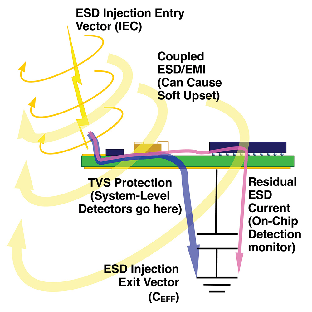
- Be the Bolt: Identify the entry/exit vector(s) of concern. Find a place to attach a voltage, current, or near-field probe to the discharge path in order to trigger your detector. (See Figure 1.)
- Circuit Modifications: Integrate the technology’s response mechanisms into your circuitry, ensuring that they can be triggered promptly upon ESD event detection.
- ESD Event Simulation: Simulate ESD events of varying magnitudes and polarities to verify that the embedded detection system reliably detects and responds to them. Do not waste time inventing your own ESD pulse model. Select the appropriate one from the dozens of industry-developed ESD pulse spice models available in the literature.
- Response Testing: Ensure that the system’s response time and level ranges meet the requirements of your application.
- False Positive/Negative Analysis: Evaluate the system’s performance in terms of false positives (incorrectly detecting an ESD event due to non-ESD EMI, for example) and false negatives (failing to detect a genuine ESD event).
One problem of cutting-edge chip-level characterization has been the scarcity of early functional samples of “golden” qualification chips and early validation system boards. Many of these chips and evaluation boards are critically allocated to software development or other functional requirements and cannot be sacrificed for ESD or other potentially destructive transient testing.
Embedded transient scanning detectors may be designed to trigger at various levels of applied stress and may, therefore, provide an early “warning track” of imminent failure. Traditional step-testing of a system can begin from a harmless starting point and be increased incrementally until near-destructive levels are detected, allowing testing to be aborted before damage occurs. The guardbanding of the target robustness level can be validated in this way without destroying the device.
- ESD Generator Testing: Use ESD generators to emulate ESD events and verify that the embedded detection system responds appropriately. Test under various conditions, including different magnitudes and polarities of ESD strikes. Carefully document the detector levels and ranges that correspond to different strike levels applied at different injection points.
- Multi-strike ESD Robustness Testing: Subject the semiconductor chip to a series of ESD events to determine its robustness and ability to continue functioning under ESD stress. While some stress levels will precipitate instantaneous damage, other types of latent damage can accumulate after repeated strikes at much lower levels.2
- Temperature and Voltage Testing: Test the embedded detection system under extreme temperature and voltage conditions to ensure its reliability across different operating environments.

In Parts 2 and 3, we’ve provided engineers and designers with an overview of embedding ESD detection in their products and processes. Embedded ESD detection gives you more visibility and flexibility, allowing you to optimize cost, enhance performance, and bolster robustness as semiconductor technology advances.
- J. Dunnihoo (author) and Simona Ceccarelli (illustrator), TSSOP gets ZAPPED! with Static Electricity, Pragma Media, 2019
- I. Laasch, H-M. Ritter and A. Werner, “Latent damage due to multiple ESD discharges,” EOS/ESD Symposium, Anaheim, CA, 2009, pp. 1-6.