NSI/ESDA/JEDEC JS-002 [1] specifies how to test and qualify a product for a factory CDM event. The document is intended for the testing of packaged devices. Thus, CDM testers in the industry have mechanical stages and contact pins that are oriented towards products in packages with pin pitches typical of today’s package sizes. With shrinking footprints and increasing integration (for example, flip chip or wafer level chip scale packaging), bare die are being sold to original equipment manufacturers (OEMs). OEMs are asking the IC manufacturers to give a CDM rating for these packageless products. However, the existing CDM testers introduce issues when considering the testing of small form factor die. Additionally, there are products that have very low withstand voltages for CDM, and the traditional CDM testers do not produce reliable waveforms for voltages below 100V. This column discusses some of the issues with Field-Induced CDM (FICDM) testing, which is troublesome for small form factor and interface die.
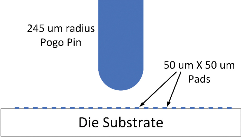
The flip chip products pose problems for CDM testing. One problem is that the pitch of these bumps is so small that the pogo pin of an FICDM tester cannot contact one bump at a time. In addition, these die are small, which makes it difficult to hold the device in place on a FICDM tester.
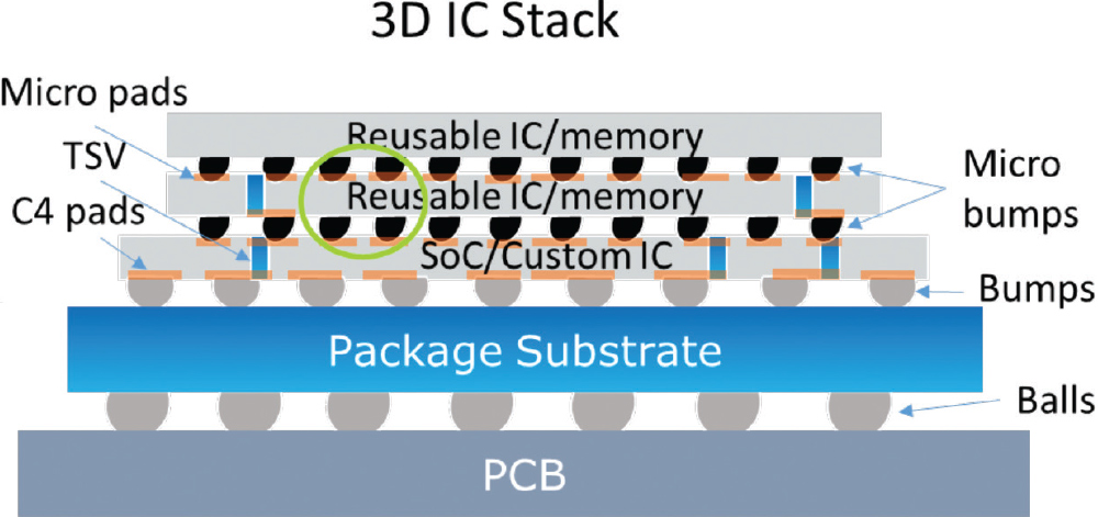
Traditionally, multi-die packages have separate ICs inside the package. Therefore, the solder ball sizes and spacings were the same size and pitch as a package substrate. With the desire for increased connections between the different die in the package, manufacturers have developed a variety of 2.5D and 3D packaging solutions. Figure 1 illustrates a 3D IC stack.
- FICDM testers may struggle to probe the small pads or bumps.
- The use of a modified pogo may change the ESD stress.
- Air discharge cannot be guaranteed at low voltages.
- A pointed pogo pin tip can change the nature of the arc due to the electric field enhancement at the sharp tip.
- The positional encoder and servomotor robotics of CDM testers may not be accurate enough to optimally position the pogo pin over the bump.
There exist several viable options for bare-die CDM testing. There is no consensus on which one of these options is the best. The follow-on papers to this introduction will review what has been used in the industry, along with the pros and cons of each approach.
- Robert Ashton (retired)
- David Epps (AMD)
- Jared Floyd (ESDEMC)
- Wei Huang (ESDEMC)
- David Klien (pSemi)
- Tom Meuse (Thermo Fisher)
- Kathleen Muhonen (Qorvo)
- Friedrich sur Nieden (Infineon)
- Paul Phillips (Phasix)
- Michael Reardon (ESDEMC)
- Masnori Sawada (Hanwa)
- Jasmine Shen (ESDEMC)
- Marko Simicic (IMEC)
- Heinrich Wolf (Fraunhofer)
- ANSI/ESDA/JEDEC JS-002, Charged Device Model (CDM) – Device Level, EOS/ESD Association.