Testing of single bare dies using the field-induced CDM (FICDM) setup according to JS002 [3] standard is not possible. One issue is the difficulty of touching bare die pads with the pogo‐pin, whose diameter can exceed the pad size. Moreover, FICDM testing at voltages below 20 V leads to unstable waveforms. The standardized testing setup does not reflect the real capacitance and peak current relationship due to the small dimensions and thickness of the dies, which affect CDM peak currents, rise times, and pulse widths. There are arguments for using alternative testing methods, such as CCTLP, to enable the testing of bare dies [4].
These challenges are addressed by an alternative approach that transforms CDM charging voltage into current using the parameter device volume and effective capacitance Ceff. This transformation [5] facilitates alternative testing methods like Capacitively Coupled Transmission Line Pulsing (CCTLP). The capacitance is proportional to the product dimensions. Besides the area, the thickness of a die influences the peak current.
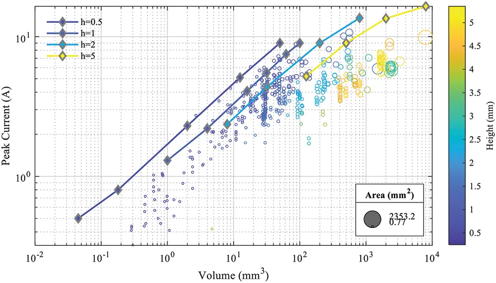
Figure 1 shows the relation between device dimensions in volume versus the Ceff in a CDM tester. The solid lines represent the upper limit for a device dimension coming from the static capacitance simulation with fully metallic cuboids. The products always lay below the solid line, and the respective height is color-coded. The simulation shows that height itself has only an influence if the height itself surpasses the side length of the fully metallic body. For packaged devices, the experiments show a contrary effect in a way that the capacitance decreases with height. This is because the slimmer the packages, the more percentage of conductive material they include that contributes to the device capacitance.


- D. Johnsson, P. Tamminen, T. Viheriäkoski, and H. Gossner, “Discharge Waveforms of Emulated Die-to-Die ESD Discharges,” 2023 45th Annual EOS/ESD Symposium (EOS/ESD), Riverside, CA, USA, 2023, pp. 1-9.
- G. Fellner, D. Pommerenke, L. Zeitlhoefler, and F. zur Nieden, “Transmission Line Based CDM ESD Current Target to Overcome Bandwidth Limitations,” International Symposium and Exhibition on Electromagnetic Compatibility EMC Europe 2024, Bruges, Belgium, 2024.
- ANSI/JEDEC/ESDA, “Joint Standard for Electrostatic Discharge Sensitivity Testing – Charged Device Model,” JS-002, 2018.
- ANSI/ESD, Standard Practice for Electrostatic Discharge Sensitivity Testing – Charged Device Model (CDM) Testing – Component Level – Capacitively Coupled – Transmission Line Pulsing as an Alternative CDM Characterization Method, SP5.3.4-2022.
- L. Zeitlhoefler, T. Lutz, F. Zur Nieden, K. Esmark, and R. Gaertner, “Voltage to Current Correlation for CDM Testing,” 2023 45th Annual EOS/ESD Symposium (EOS/ESD), Riverside, CA, USA, 2023, pp. 1-11.
- M. Johnson, R. Ashton, and S. Ward, “FCDM Measurements of Small Devices,” 2009 31st EOS/ESD Symposium, Anaheim, CA, USA, 2009, pp. 1-8.
- L. Zeitlhoefler, F. Z. Nieden, K. Esmark, and R. Gaertner, “Limitation of CDM Testing for Small Devices,” 2022 44th Annual EOS/ESD Symposium (EOS/ESD), Reno, NV, USA, 2022, pp. 1-9
- C. Eichenseer, G. Langguth, R. Gaertner, F. Z. Nieden, L. Zeitlhoefler, and S. Kokorovic, “Fast Transient ESD Protection at RF Pins,” 2023 45th Annual EOS/ESD Symposium (EOS/ESD), Riverside, CA, USA, 2023.