EMC concepts explained
Evaluation of EMC Emissions and Ground Techniques on 1- and 2-layer PCBs with Power Converters
Part 2: DC/DC Converter Design with EMC Considerations
T

his is the second in a series of articles devoted to the design, test, and EMC emissions evaluation of 1- and 2-layer PCBs that contain AC/DC and/or DC/DC converters and employ different ground techniques [1]. In this article, we first present a top-level schematic of an overall system and then focus on a systematic approach to a DC/DC converter design. Several EMC considerations are addressed at the schematic level, and recommended design improvements are provided to reduce the risk of failures during testing.

1. Introduction
Most hardware designs begin with a baseline schematic based on the Integrated Circuit (IC) supplier’s guidelines and application notes. These application notes show examples of how to implement the devices along with guidance on how to design and eventually translate the design into a Printed Circuit Board. The level of EMC consideration provided in the vendor design resources and datasheets of each component varies significantly and may not be comprehensive enough to ensure EMC compliance in all industries where the devices could be used. The staff at E3 Compliance will typically perform an EMC design review on designs in the early stages of development. The purpose of the design review is to identify EMC concerns or risks against the requirements and recommend design improvements to prevent EMC failures during testing. This is an important step to a successful product development process that helps streamline the pre-compliance testing where final EMC issues are detected and resolved before EMC Compliance testing.

In this article, we present the schematic for the overall system, followed by a detailed schematic of a DC/DC SMPS. The design of a 24V-to-3.3 V DC/DC converter follows the design process philosophy where we start with a baseline functional schematic based on the IC manufacturer specifications. These specifications usually do not fully address non-functional concerns like thermal or EMC issues. We, therefore, address these issues and recommend design improvements to prevent failures during testing.

We conclude with a brief description of the next article.

2. Schematics and Design Requirements
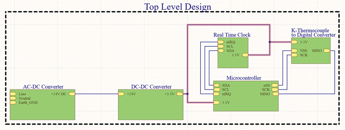
Figure 1 shows the top-level system schematic.
Top-level schematicFigure of
Figure 1: Top-level schematic
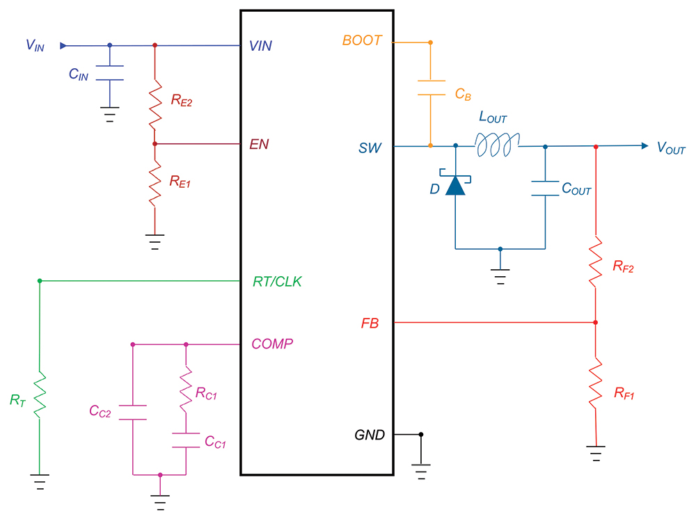
In this article, we focus on the DC/DC converter shown in Figure 2.

In our design, we use Texas Instruments TPS54360B step-down regulator with integrated high side n-channel MOSFET, [2]. The device implements constant frequency, current-mode control.

Figure of DC-DC converter simplified schematic
Figure 2: DC-DC converter simplified schematic
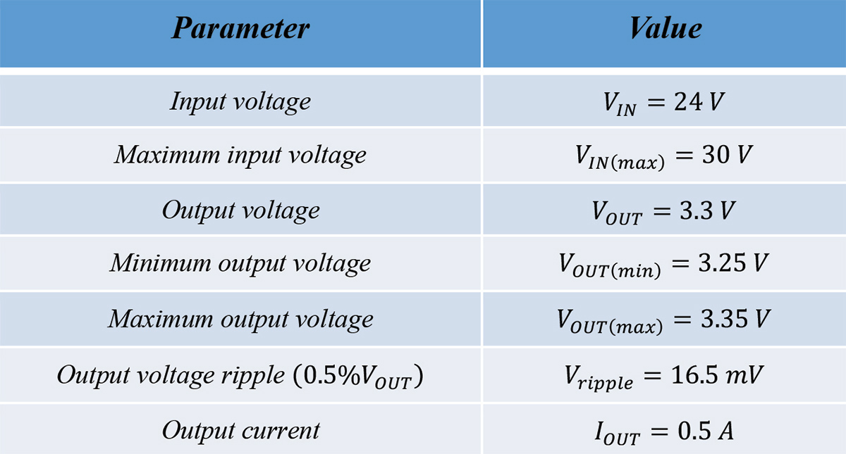
To begin the design process, the design requirements must be set. These are shown in Table 1.

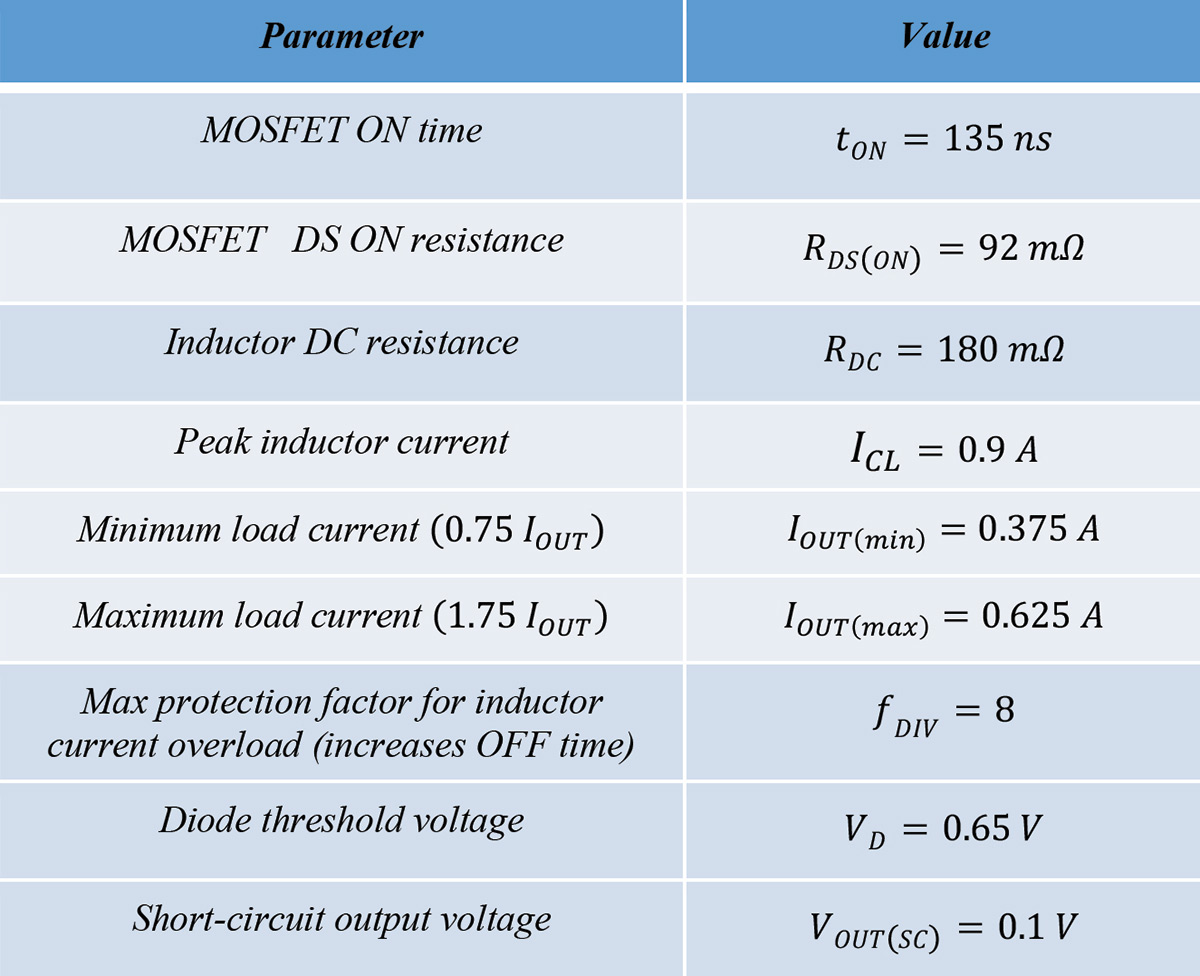
Additional assumptions and design constraints are listed in Table 2.

Table of Design requirements
Table 1: Design requirements
Table of Design constraints
Table 2: Design constraints
3. Design Process
In this section, we describe the detailed design process for each regulator subsystem.
3.1. Switching Frequency
Selecting the switching frequency is the first step in the design. According to the device specification, the upper limit on the switching frequency is determined from two equations:
equation
equation
equation
equation
The operating frequency should be lower than the lowest of the two values predicted by Equations (1) and (2). In our design, targeted switching frequency fSW = 600 kHz.

The switching frequency is adjusted using a (timing) resistor to ground connected to the RT/CLK pin. The timing resistance for a given switching frequency is determined from:

equation
The switching frequency corresponding to the nominal value of RT = 160 kΩ is calculated from
equation
3.2. Output Inductor
The minimum value of the inductor current is obtained from
equation
KIND = 0.3 in Equation (5) comes from the regulator datasheet. In our design, we chose Wurth 744053330 inductor with a nominal value of LOUT = 33 μH.

The inductor ripple current is calculated from

equation
The inductor ripple current is part of the current mode PWM control system, and the suggested minimum value of the ripple current for a 5 V regulator is 150 mA. Since we are designing a 3.3 V regulator, the value 147 mA is acceptable.

The inductor RMS current is calculated from

equation
The peak inductor current is obtained from
equation
The Würth 744053330 inductor has a rated current of 900 mA and the saturation current of 750 mA, and thus the calculated values are well within these limits. (The maximum output current of 625 mA shown in Table 2 is also within these limits).
3.3. Output Capacitor
The output capacitor needs to satisfy several criteria. The first is the allowable change in the output voltage for a maximum change in the load current.
equation
The output capacitor must also be sized to absorb the energy stored in the inductor when transitioning from a high to a low load current. This value is obtained from
equation
The minimum output capacitance needed to satisfy the output voltage ripple is obtained from
equation
The output capacitance should be larger than the largest value calculated in Equations (9) through (11). Additionally, we need to account for the derating of the output capacitor; thus, let’s double the value given by Equation (10) to arrive at COUT(min) = 49.6 μF. This value will be later used when designing the compensation network.

To account for the safety margin in our design, we chose two output capacitors in parallel, each of the value COUT = 47 μF.

Maximum ESR of the output capacitor is calculated from

equation
In our design, we chose Murata capacitor GRM32ER71A476KE15L with an ESR of 3 at 100 kHz, which is well below the maximum ESR predicted by Eq. (12).
3.4. Catch Diode
The regulator requires an external catch diode between the SW pin and GND. The diode must have a reverse voltage rating equal to or greater than VIN(max). The peak current rating of the diode must be greater than the maximum inductor current. The diode must also have an appropriate power rating. The power dissipation of the diode is calculated from
equation
where cT is junction capacitance. We chose a Schottky diode B260S1F from Diodes Incorporated. It is rated at the reverse voltage of 60 V, peak current of 2 A, VD = 0.65 V, cT = 75 pF.

Thus, the power dissipation of the diode is

equation
and is well below the power threshold for the rated voltage and current values.
3.5. Input Capacitor
The regulator requires a high-quality ceramic type X5R or X7R input capacitor with at least 3 µF of effective capacitance. The voltage rating of the input capacitor must be greater than the maximum input voltage.

In our design, we use two Murata GCJ32DR72A225KA01L, 2.2 µF, 100V, ceramic capacitors in parallel.

3.6 Bootstrap Capacitor
A bootstrap capacitor between the BOOT and SW pins is needed to provide the gate voltage to drive the high-side MOSFET. The recommended value is 0.1 µF. TI recommends a ceramic capacitor with X7R or X5R grade dielectric with a voltage rating of 10 V or higher.

In our design we use 0.1 µF, 50 V Murata GCJ188R71H104KA12D capacitor.

3.7. Undervoltage Lockout
According to the specifications, the input voltage range of the regulator is 4.5 V – 60 V. In our application, the input voltage to the regulator is 24 V (VIN). The regulator is enabled when the input voltage (VIN) rises above 4.3 V and disabled when this voltage drops below 4.3 V. The undervoltage lockout (UVLO) of 4.3 V can be adjusted with two resistors (forming a voltage divider) connected to EN pin, as shown in the schematic.

When adjusted to a non-default value of 4.3 V, the undervoltage lockout (UVLO) has two thresholds, one for power up when the input voltage is rising (UVLO start), and one for power down when the input voltage is falling (UVLO stop).

In our application, we chose UVLO start or VSTART = 8 V and UVLO stop or VSTOP = 6.25 V. Then the values of the two resistors are calculated as follows. The value of the resistor between E V and VIN, RUVLO1, is obtained from

equation
IHYS is internally set to 3.4 µA. Thus, in our design,
equation
The value of the resistor between E V and GND, RUVLO2, is obtained from
equation
IHYS is internally set to 1.2 µA. Thus, in our design,
equation
3.8. Feedback Pin
The FB pin monitors the output voltage by comparing it to the internal value of 0.8 V. The output voltage is set by a resistor divider from the output node to the FB pin. The current flowing through the feedback network should be greater than 1 µA to maintain the output voltage accuracy. The resistors comprising the voltage divider should have 1%, or better, tolerance.

If a low-side resistor, RLS = 10 kΩ is used, then the high side resistor value, RHS, is obtained from

equation
In our application, VOUT = 3.3 V resulting in RHS = 31.25 kΩ. The resulting current in the feedback circuitry is 80 µA.
3.9. Compensation Network
The COMP pin is connected to the frequency compensation connected to the COMP pin (see Figure 2). The compensation network internally provides input to the PWM circuitry, which controls the switching of the SW node and thus controls the current to the load. Specifically, the COMP pin voltage controls the peak current on the high side MOSFET.

To design the compensation network, we follow the procedure outline in the regulator specifications. First, several frequencies are calculated.

equation
equation
equation
equation
The lower of the two values fCO = fCO2 in Equations (22) and (23) will be used.

The resistor RC1 in the compensation network is calculated from

equation
From the regulator specifications, we use
equation
Thus,
equation
The capacitor CC1 in the compensation network is calculated from
equation
The capacitor to ground, CC2, in the compensation network is calculated from two different equations and the larger value is chosen.
equation
equation
4. Complete Regulator Circuitry
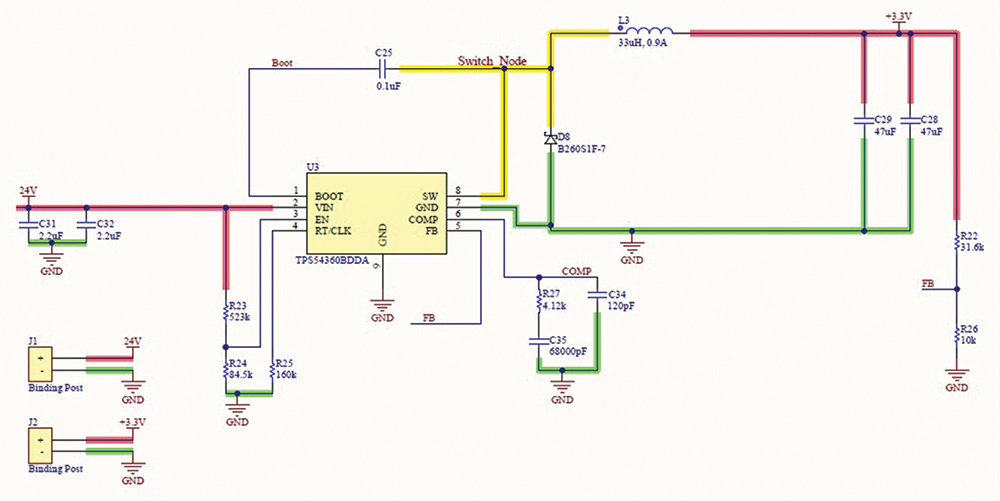
Figure 3 shows the complete circuitry of the designed regulator. Red-colored nets represent power input and output. Yellow-colored nets represent the switch node. Green-colored nets represent ground.
Figure of DC-DC converter circuitry
Figure 3: DC-DC converter circuitry
5. EMC Considerations
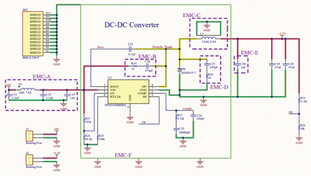
An EMC design review was performed to identify high-risk areas to meeting emissions requirements. During the review, a number of additional components were identified for filtering, damping switching effects, inductor technology, and shielding options. The schematic shown in Figure 3 was modified by superimposing the EMC considerations, shown as dashed boxes labeled A through F in Figure 4. The values of these EMC components are chosen based on experience but will likely need to be tuned in the laboratory through experimental measurements.
Figure of DC-DC converter circuitry with EMC considerations
Figure 4: DC-DC converter circuitry with EMC considerations
These considerations are addressed below.

EMC-A: A 1nF capacitor (C33) is added on the Vin pin (U1.2) for high-frequency decoupling to reduce the amount of high-frequency energy generated by the DC-DC Converter that can conduct into the 24 V bus. Additionally, a π filter, [3], is constructed by adding a 1 µH inductor (L4) between the two input capacitors (C31 and C32).

EMC-B: A snubber circuit (series Resistor R19 & Capacitor C26) is added from SW Node (U1.8) to Vin (U1.2) because the Internal MOSFET is placed between these pins. This snubber is used to control the ringing from the internal MOSFET that results from the step response to the RLC network.

EMC-C: The Würth Elektronik inductor (L3) may be replaced with a Vishay IHLP inductor which is magnetically shielded or an IHLE inductor which is E-Field shielded to reduce radiated and conducted emissions further.

EMC-D: A snubber circuit (series Resistor R20 & Capacitor C27) is added across the catch diode to reduce ringing across the diode junction [4].

EMC-E: A 1nF capacitor (C30) is added near the inductor (L3) on the 3.3 V bus to filter high-frequency noise from conducting out onto the 3.3 V bus.

EMC-F: A shield (SH1) may be added if the PCB layout and EMC components are not successful to reducing the emissions from the DC-DC Converter. This may be needed in some instances where the EMC requirements are very stringent or the supply may be closely co-located to sensitive receivers.

These EMC components are designed into the first prototype as optional components that will be evaluated during emissions testing. The EMC performance may have trade-off decisions to make with regard to other requirements such as thermal, reliability, manufacturability, and cost. An example would be selecting the snubber values to optimize the EMC and thermal performance. Not all of the EMC components will likely be needed, and efforts will be made to remove the unneeded components to optimize cost.

6. Future Work
The next step will be to fabricate and build the DC/DC converter PCB. Functional performance and the radiated and conducted emissions subsequently will be evaluated and discussed. Additionally, a summary of chosen EMC components required to gain compliance shall be reviewed.
References
  1. Adamczyk, B., Mee, S., Koeller, N, “Evaluation of EMC Emissions and Ground Techniques on 1- and 2-layer PCBs with Power Converters – Part 1:Top-Level Description of the Design Problem,” In Compliance Magazine, May 2021.
  2. https://www.ti.com/product/TPS54360B
  3. Adamczyk, B., Gilbert, B., “MC Filters Comparison Part II: π and T Filters,” In Compliance Magazine, January 2020.
  4. Mee, S., Teune, J., “Reducing Emissions In The Buck Converter SMPS,” IEEE EMC Symposium Record, 2002.
Share this story:
Bogdan Adamczyk headshot
Dr. Bogdan Adamczyk is professor and director of the EMC Center at Grand Valley State University (http://www.gvsu.edu/emccenter) where he regularly teaches EMC certificate courses for industry. He is an iNARTE certified EMC Master Design Engineer. Prof. Adamczyk is the author of the textbook “Foundations of Electromagnetic Compatibility with Practical Applications” (Wiley, 2017) and the upcoming textbook “Principles of Electromagnetic Compatibility with Laboratory Exercises” (Wiley 2022). He can be reached at adamczyb@gvsu.edu.
Scott Mee smiling in a professional headshot
Scott Mee is a co-founder and owner at E3 Compliance which specializes in EMC & SIPI design, simulation, pre-compliance testing and diagnostics. He has published and presented numerous articles and papers on EMC. He is an iNARTE certified EMC Engineer and Master EMC Design Engineer. Scott participates in the industrial collaboration with GVSU at the EMC Center. He can be reached at scott@e3compliance.com.
Nick Koeller smiling in a professional headshot
Nick Koeller is an EMC Engineer at E3 Compliance which specializes in EMC & SIPI design, simulation, pre-compliance testing and diagnostics. He received his B.S.E in Electrical Engineering from Grand Valley State University and is currently pursuing his M.S.E in Electrical and Computer Engineering at GVSU. Nick participates in the industrial collaboration with GVSU at the EMC Center. He can be reached at nick@e3compliance.com.