his is the second of three articles devoted to the design, test, and EMC immunity evaluation of multilayer PCBs containing analog circuitry. The first article presented a top-level block diagram description of the design problem under research [1,2]. This article is devoted to the RF immunity testing according to the ISO11452-11 Radiated Immunity Reverberation Method standard from 400MHz – 1GHz, up to 100V/m. As a reminder, two analog measurements are present on the PCB. The first analog measurement captures analog temperature values from a Negative Temperature Coefficient (NTC) thermocouple at the end of a short harness. The second analog measurement captures the analog voltage of 12 volts connected at the banana jack terminals of the PCB. Both sets of values are processed by the microcontroller and reported to the test engineer outside the chamber via Universal Asynchronous Receiver Transmitter (UART) and fiber optic communications for isolation. However, for this article, only analog temperature measurements are presented and discussed.
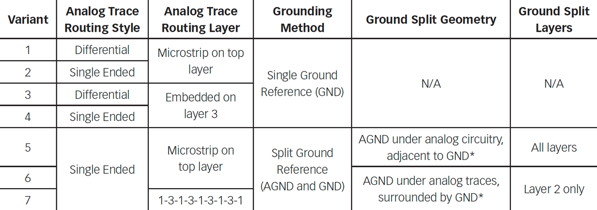
In this study, there are seven design variants that all contain a similar schematic but implement different PCB layout techniques (see [1] for the details). The design variants are described in Table 1.
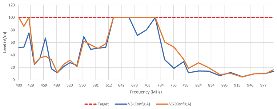
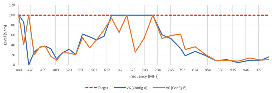
Next, Variant 6 was tested, and the results were compared to those of Variant 5. The comparison is shown in Figure 6.
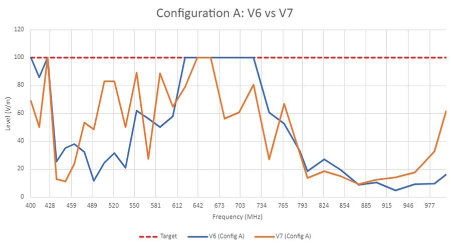
Observations: Jumping the analog traces from Layer 1 to 3 (Variant 7) introduces regions where one variant outperforms the other. Variant 7 shows better immunity in the lower frequency range, while Variant 6 is better in the mid-frequency range. Our experience has shown that jumping layers should be avoided as it introduces anomalies in an unpredicTable frequency range.
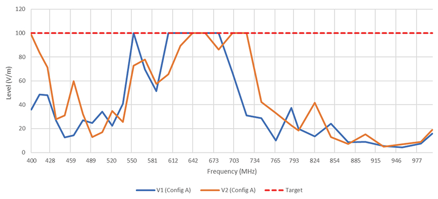
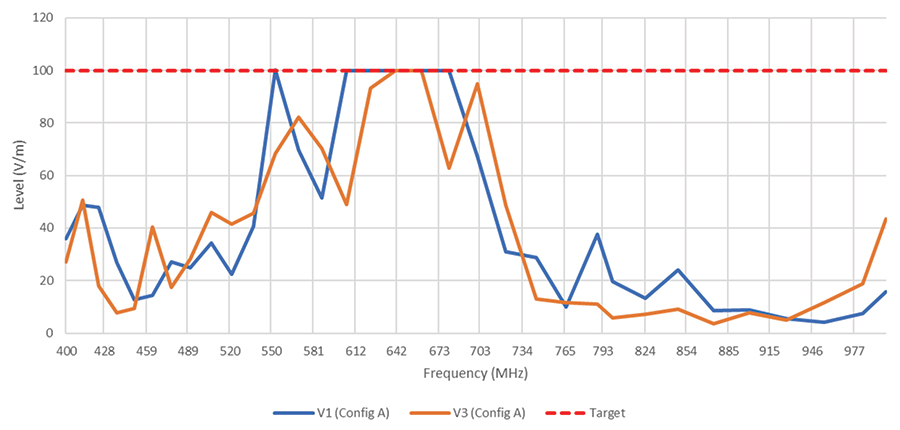
Figure 8 on page 44 compares the test results for Variant 1, Configuration A vs. B.
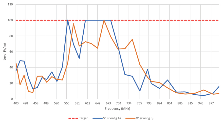
Figure 9 on page 44 compares the test results for Variant 5, Configuration A vs. B.
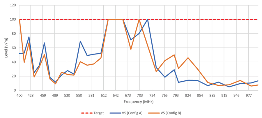
Figure 10 on page 44 compares the test results for Variant 6, Configuration A vs. B.
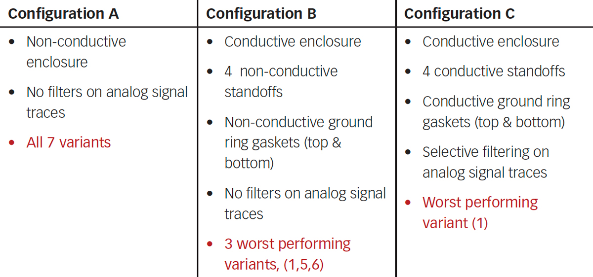
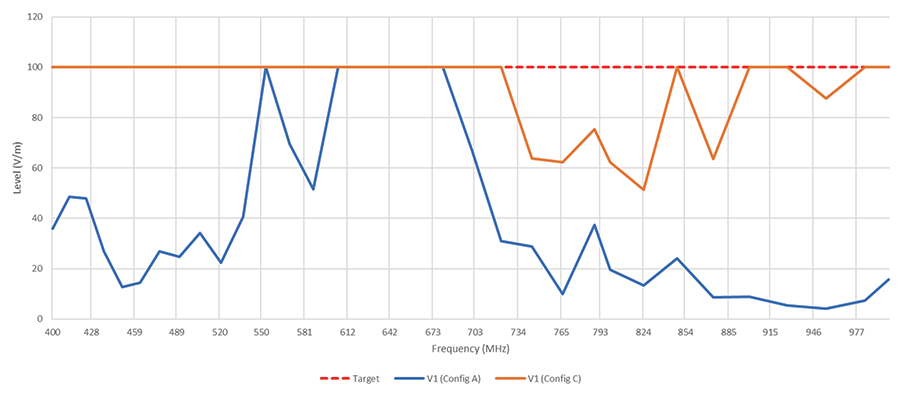
Observations: Variant 1 in Configuration C performed dramatically better than Configuration A over a wide band of frequencies from 400MHz to 1000MHz. Improvements were made due to the shielded enclosure, conductive standoffs, conductive gaskets, and selective filtering components on the analog lines. Since Configuration B (shielded enclosure, non-conductive standoffs) didn’t provide as much benefit as Configuration C, the added conductive gaskets, conductive standoffs, and component filtering likely provided the most benefit.
5. Future Work
- Baatar, B., Costantino, C., Morey, R., Muldowney, C., EMC PCB Design Study, GVSU senior project sponsored by E3 Compliance, LLC.
- Adamczyk, B., Mee, S., Baatar, B., “Evaluation of PCB Design Options using a Multilayer PCB – Part 1: Top-Level Description of the Design Problem,” In Compliance Magazine, May 2022.