n this article, we discuss the PCB layout considerations and the design of the reference return paths for the one- and two-layer boards.
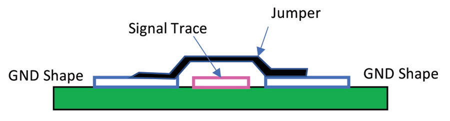
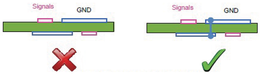
Visualizing the loop areas allows the designer to identify ways to reduce the size and cross-sectional area of the loops, thus reducing the inductance and high-frequency impedance. In single-layer PCB designs, there is fierce competition for copper routing real estate as all routes need to be completed on a single layer. In this setting, we don’t have the luxury of a reference return on the secondary side of the PCB. We rely on prioritizing the reference return connections between critical points and loop areas are often much larger than we would like to see. This can drive the need for additional decoupling capacitors, filter components and ‘jumper’ components to ‘stitch’ reference returns back together across other trace routes. Figure 1 shows an example of a jumper used to ‘stitch’ the ground areas back together across a signal trace route.
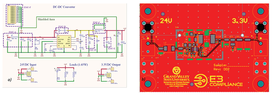
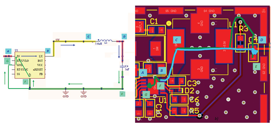
During the design of the DC-DC Buck converter that has been discussed over the last three articles [x], the reference path design has been the main concern and will continue to be a concern of this study. The schematic and layout of this DC-DC Buck converter are shown in Figure 3. Figure 3a shows the power and signal traces as well as the reference return conductors (highlighted in green). Figure 3b shows the corresponding layout traces and the ground pads (highlighted in green).
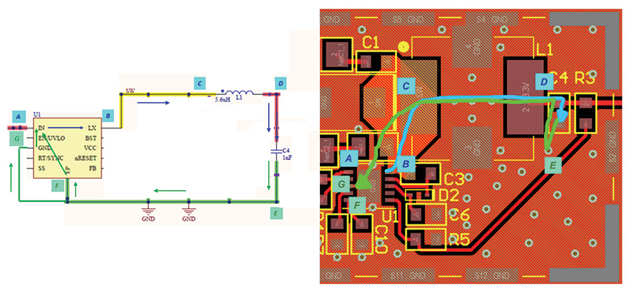
Let’s demonstrate this by looking at one of the output filtering capacitors shown in Figure 4. The forward path of the current is A-B-C-D, and the current return path is E-F-G.
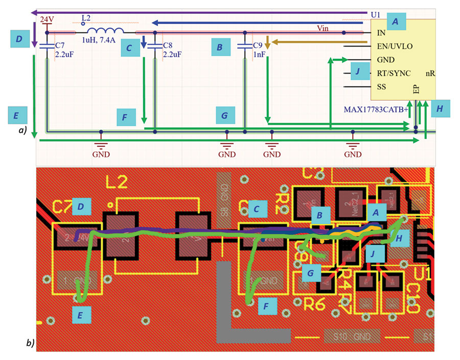
With a completely solid GND plane, the currents will have no issues returning directly under the forward path, but in many practical designs this is just not possible. Generally, at least a couple of traces may need to be routed in the GND plane, especially on a two-layer board. The output section of this DC-DC power supply was modified to allow us to analyze how the current might return to the source when the ideal return path is broken by a trace in the GND plane. This modified output section is shown in Figure 5 on page 44.
Next, let’s look at the input filtering section shown in Figure 6 on page 45.
As the circuit complexity increases, it becomes challenging to visualize all possible high-frequency current paths. What can be done then?
This is where the application of some good EMC rules of thumb can help. Here are several that we have identified over the years by working on power converters and solving EMC emissions issues:
- Wherever possible, keep a solid reference plane on the secondary (or adjacent) layer
- Place decoupling and by-pass capacitors as close to the IC pins as possible
- Ensure short connections and provide adequate reference via connections adjacent to component reference (GND) pins to ensure a low impedance path (smallest loop area)
- Place all high di/dt components on the same layer of the PCB and in close proximity
- Place optional snubber components (series R C) across the internal switch and free-wheeling diode. Locate components in close proximity with short connections.
- Fill with reference area fill beneath switching components (ICs, inductors, etc.)
- Adamczyk, B., “Alternative Paths of the Return Current,” In Compliance Magazine, May 2017.
- MAX5022 Evaluation Kit, MAX5022, Rev 3, Maxim Integrated, 2021, https://datasheets.maximintegrated.com/en/ds/MAX5022EVKIT.pdf.


