his is the fifth article in a series of articles devoted to the design, test, and EMC emissions evaluation of 1- and 2-layer PCBs that contain AC/DC and/or DC/DC converters, and employ different ground techniques [1-4]. In this fifth article, we are still focused on the DC/DC power converter board (2-layer PCB). In this article, we evaluate the implementation of several EMC countermeasures and present the conducted emissions results, for both voltage and current methods, according to CISPR25 Class 5 limits.
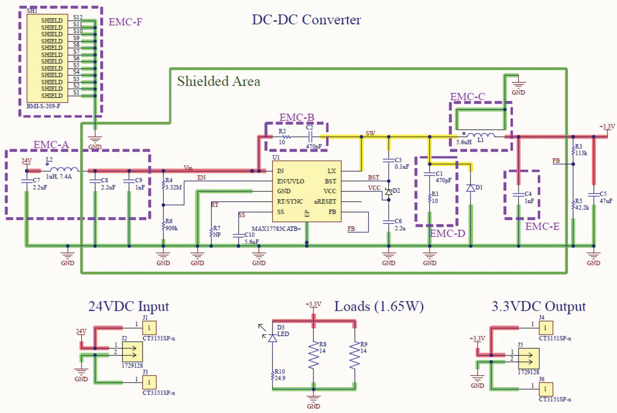
In the first article in the series, [1], we defined the overall design problem. The second article, [2], focused on the details of the 2-layer DC/DC converter design. The third article [3] presented the radiated and conducted emission results from the baseline design, which did not contain any EMC countermeasures. The results showed multiple failures in both radiated and conducted emissions. The fourth article [4] presented a systematic approach to improve these radiated failures by populating the PCB with optional EMC countermeasures on component pads that have already been designed into the PCB layout and showing their impact on the radiated emissions. The EMC countermeasures are illustrated in Figure 1 as purple dashed boxes labeled EMC-A through EMC-F.
This article discusses the impact of these countermeasures on the conducted emissions results using both the voltage and the current methods. The voltage method results are discussed first, followed by the current method results. The article concludes with a brief description of what can be expected in the next article in the series.
The voltage method results are shown only for the supply line, as the ground line results were similar.
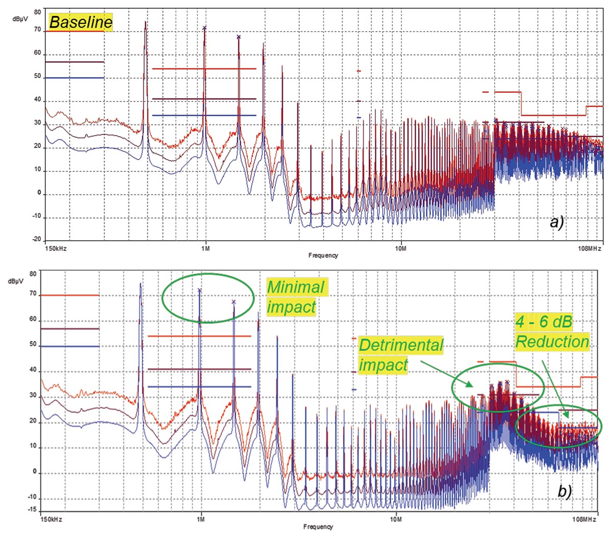
Conducted emissions were measured in the frequency range of 150 kHz – 108 MHz. The baseline results (Figure 2a) show a high level of emissions in the 1 – 2 MHz and 25 – 100 MHz bands. To attempt to reduce these emissions two capacitors C9 = 10 nF (EMC-A) and C4 = 10 nF (EMC-E) were populated. The conducted emissions measurement taken with these countermeasures populated is shown in Figure 2b. See Figure 6 in the third article in the series for a reference legend to interpret plots in this article [3]. This figure was not duplicated in this article in order to save space.
The 10nF capacitors are meant to help filter the noise in higher frequencies. As the plot in Figure 2b shows, the capacitors increase the conducted emissions in the frequency range of 25 MHz – 40MHz, and decrease the conducted emissions in the frequency range of 40 MHz – 100MHz. The additional capacitors have minimal impact on the conducted emissions in the 1 MHz – 2 MHz band. The 10nF capacitors are kept on the board for the next two sections as they had a positive impact in the 40 MHz – 100 MHz band.
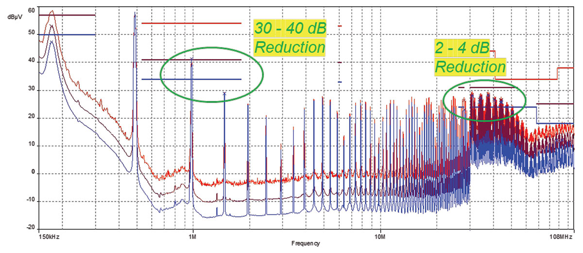
Next, we targeted the conducted emissions using an input filter. A 1 µH input inductor, L2 (EMC-A), was placed on the input to create a PI filter with the input capacitors. The conducted emissions measurement taken with this countermeasure in place is shown in Figure 3.
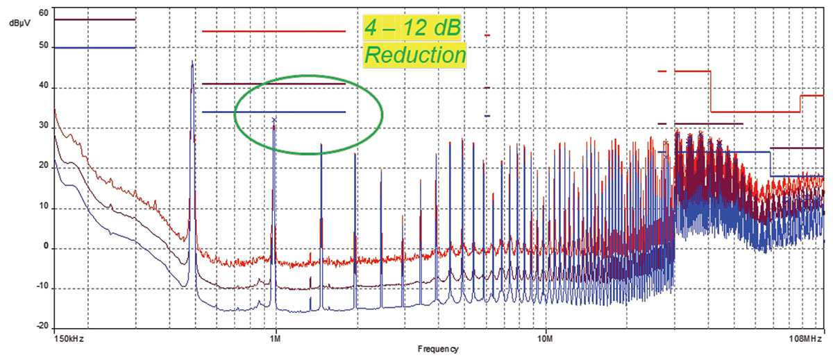
As Figure 3 shows, the inductor had a substantial improvement in the emissions in the 1 – 2 MHz range; additionally, it reduced the higher frequency emission by 2 – 4 dB compared to Figure 2b. To further reduce the emissions around 1 MHz, the input inductor L2 was changed to 3.3 µH. The emission results are shown in Figure 4.
As Figure 4 shows, an additional 4 -12 dB reduction was achieved in the lower frequency range compared to Figure 3.
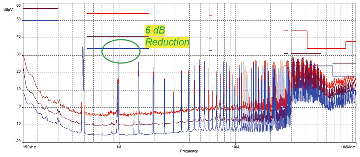
Next, we added two additional 2.2µF input capacitors, C7 and C8 in order to increase the impedance of the input PI filter by lowering the frequency of the low pass filter. The emissions results are shown in Figure 5.
As Figure 5 shows, an additional 6 dB reduction was achieved around 1 MHz compared to Figure 4.
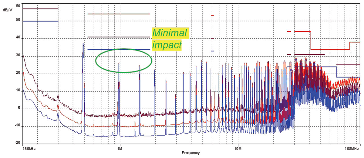
Next, the input inductor L2 was changed back to 2.2 µH IHLP magnetically shielded inductor. The emission results are shown in Figure 6.
As Figure 6 shows, the change from 3.3 µH to 2.2 µH had virtually no impact, as compared to Figure 5. This suggests that the increase in capacitance on C7 and C8 offers more improvement and the increase in inductance from 2.2uH to 3.3uH has a negligible impact, and therefore, we retained the 2.2 µH inductor in our design.
Next, the switching inductor, L1 (EMC-C), was changed to a Vishay 3232 IHLE 5.6 µH. These inductors have an integrated E-field shield that is tied to ground on two sides of the inductor. The conducted emission results are shown in Figure 7.
As the plots show, the inductor had a substantial impact in the 40-70 MHz range. At this point, the DUT is passing CISPR 25 Class 5, and initially, this is the solution that we used and is described in the previous article. [4] However, with the additional time we have had since the previous article, we decided to evaluate some other countermeasures that would be cheaper than the IHLE inductor. This approach is often used in debugging EMC issues for industry as we first prioritize finding a solution, then optimize the PCB assembly cost as time allows.
Next, we investigated the impact of the two series RC snubbers (EMC-B and EMC-D). The IHLE 5.6uH inductor was removed and replaced by L2 = 2.2 µH IHLP magnetically shielded inductor (in order to reduce the cost). The remaining EMC components were retained.
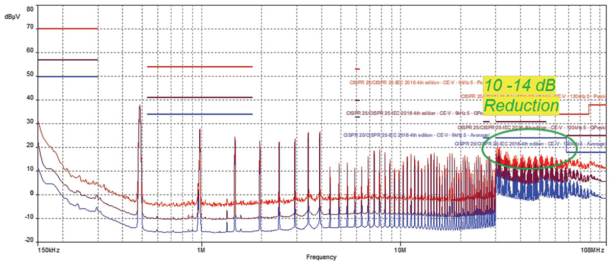
One of the snubbers was placed across the catch diode D1: R1 = 10 Ω, C1 = 470 pF (EMC-D), and the other was placed across the FET that controls the switching, R2 = 10 Ω, C2 = 470 pF (EMC-B). This FET is inside of the IC package. The conducted emissions test results are shown in Figure 8.
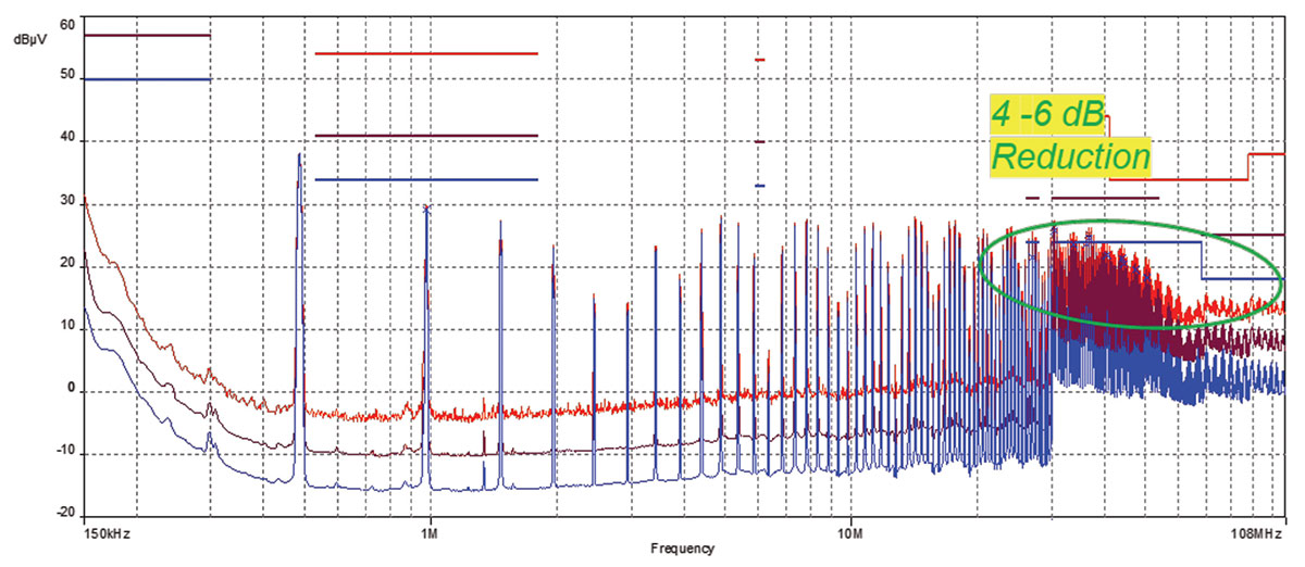
With both snubbers in place, we observe a 4 – 6 dB decrease in emissions in the 30 – 100 MHz band. Next, the snubber across the catch diode (R1 and C1) was removed while the R2 and C2 snubber was retained. The conducted emissions results are shown in Figure 9.
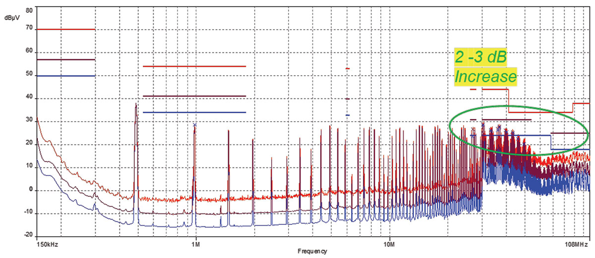
As Figure 9 shows, the removal of the catch diode snubber (R1 and C1) results in a 2 -3 dB increase in emissions in the 30 – 100 MHz band. Next, the FET snubber (R2 and C2) was removed, while the catch diode snubber (R1 and C1) was repopulated. The conducted emissions results are shown in Figure 10.
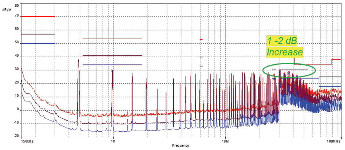
Figure 10 shows this change had a 1 -2 dB increase in the 30 – 40 MHz band, as compared to Figure 9. We, therefore, retained both snubbers.
The current method results are shown only for the 50 mm probe location, as the 750 mm results were similar.
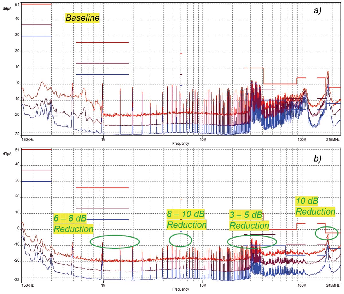
Conducted emissions were measured in the frequency range of 150 kHz – 245 MHz using the current method. The configuration tested was as follows: C9 = C4 = 10 nF, L2 = 2.2 µH, C7= C8= 2.2 µF, L1 = 5.6 µH IHLE. This is the same configuration that was used in the radiated emissions testing discussed in the previous article of this series, [4]. The conducted emissions, current method test results are shown in Figure 11.
We observe the emissions reduction across several frequency bands. This is not surprising as this configuration performed very well in the conducted emissions voltage method test.
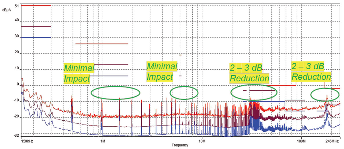
In order to address some of the higher frequency emissions, we again investigated the impact of snubbers. The IHLE 5.6uH inductor was removed and replaced by L2 = 2.2 µH IHLP magnetically shielded inductor. The remaining EMC components were retained. As it was done in the voltage method, one of the snubbers was placed across the catch diode D1: R1 = 10 Ω, C1 = 470 pF (EMC-D), and the other was placed across the switching node, R2 = 10 Ω, C2 = 470 pF (EMC-B). The conducted emissions test results are shown in Figure 12.
The addition of the two snubbers had a minimal impact on the emissions at the lower frequency ranges but resulted in about 2 – 3 dB reduction in the 20 – 30 MHz range and at the 180 MHz spike as compared to Figure 11b. This configuration does technically pass CISPR 25 Class 5, but in practice, we like to see more margin to prevent failures that can be caused by lab-to-lab variation in measurements.
Next, the FET snubber (R2 and C2) was removed, while the catch diode snubber (R1 and C1) was retained. It resulted in the increased emissions in the frequency range of 30 – 40 MHz and around 180 MHz. Subsequently, we repopulated the FET snubber (R2 and C2) and removed the catch diode snubber (R1 and C1). The result was similar.
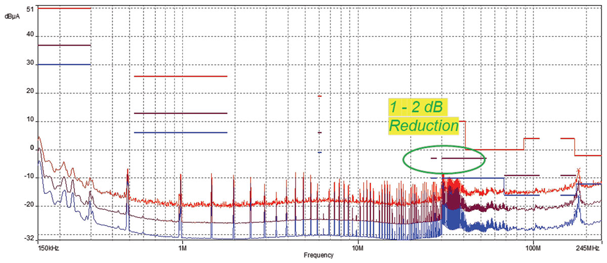
The final snubber configuration tested was with R1 = R2 = 5.6 Ω, C1 = C2 = 470 pF. The test results are shown in Figure 13.
As Figure 13 shows, this change had a positive impact in the 30 – 40 MHz range causing a 1-2 dB reduction in emissions, as compared to Figure 12. This configuration passes CISPR 25 Class 5 with 3 dB of margin.
The analysis of the conducted emissions testing and addition of EMC countermeasures show that, in large part, the failures identified in baseline testing can be mitigated through the use of front-end filtering and snubbers. However, a larger margin of passing results can be achieved by investing more in the Bill of Materials (BOM) by using an e-field shielded IHLE inductor and/or a PCB shield. Depending on the class performance desired a lower cost may be required to gain compliance with a comfortable margin.
In the next article, we will discuss the challenges of ‘grounding’ or reference layout design in single layer and 2 layer PCB designs involving DC-DC and AC-DC converters.
- Adamczyk, B., Mee, S., Koeller, N, “Evaluation of EMC Emissions and Ground Techniques on 1- and 2-layer PCBs with Power Converters – Part 1: Top-Level Description of the Design Problem,” In Compliance Magazine, May 2021.
- Adamczyk, B., Mee, S., Koeller, N, “Evaluation of EMC Emissions and Ground Techniques on 1- and 2-layer PCBs with Power Converters – Part 2: DC/DC Converter Design with EMC Considerations,” In Compliance Magazine, June 2021.
- Adamczyk, B., Mee, S., Koeller, N, “Evaluation of EMC Emissions and Ground Techniques on 1- and 2-layer PCBs with Power Converters – Part 3: DC/DC Converter – Baseline EMC Emissions Evaluation,” In Compliance Magazine, July 2021.
- Adamczyk, B., Mee, S., Koeller, N, “Evaluation of EMC Emissions and Ground Techniques on 1- and 2-layer PCBs with Power Converters – Part 4: DC/DC Converter –EMC Countermeasures – Radiated Emissions Results,” In Compliance Magazine, August 2021.


