n the rapidly evolving semiconductor industry, the shift towards Multi-Chip Modules (MCM) and Systems in a Package (SiP) is notable. These advanced assemblies comprise multiple chiplets, sensors, and optoelectronic components, which are vulnerable to Electrostatic Discharge (ESD). The complex internal architecture of MCMs and SiPs—with their internal pins and through-silicon vias—poses challenges for ESD protection in assembly processes.
During the assembly of these systems, components may be exposed to ESD stress. Established methods for assessing the Charged Device Model (CDM) [1] robustness of individual devices exist, including advanced methods such as Capacitively-Coupled Transmission Line Pulsing (CC-TLP) [2]-[7] or low-impedance contact CDM (LICCDM) [8] [9]. While CC-TLP yields reproducible results even for bare dies or wafers, it uses current to determine the robustness level. Insufficient data currently exists regarding the correlation between charging voltages in production machines and discharge currents during the assembly process. This study proposes a method to measure discharge currents during the pick and place process, aiming to link this current to a pre-charge voltage and enhance the evaluation of ESD protection requirements for internal pins.
The DCS (Figure 1) developed for this study is a compact setup designed for integration within assembly machines. It utilizes a 50 Ω microstrip line (2) terminated by a miniature pogo-pin (3). Using up to 10 thin-film resistors between the pogo-pin and ground plane, it allows to accurately measure the discharge current. The sensor’s design allows for minimal mismatch and high-frequency bandwidth.


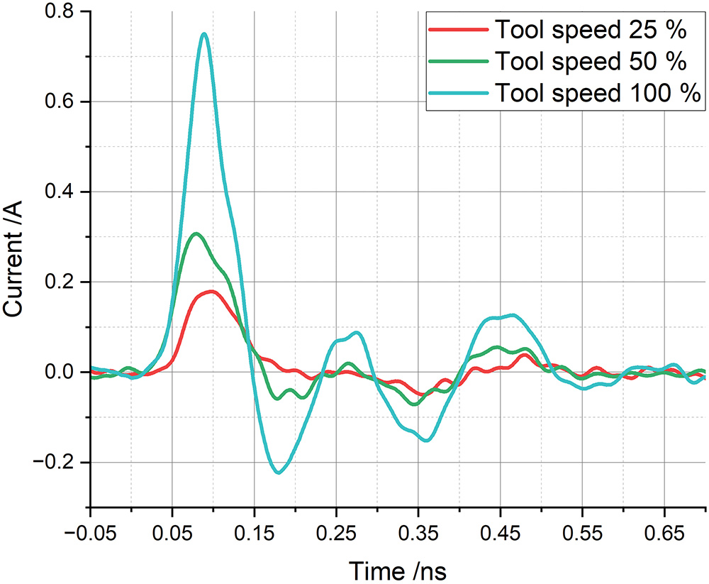
For instance, as tool speed increased, so did the discharge current, highlighting the need for careful control of assembly parameters to mitigate ESD risks (Figure 4). Additionally, the path taken by the picking tool—whether directly to the sensor or via an alignment camera—also significantly influenced the peak discharge current.
Looking ahead, further statistical data collection is essential, necessitating the development of an automated measurement setup. Efforts are already underway to create a redesigned DCS that will allow high-volume measurements.
- ESDA/JEDEC Joint Standard ANSI/ESDA/JEDEC JS-002-2022 Charged Device Model (CDM) – Device Level.
- ANSI/ESD SP5.3.4-2022, ESD Association Standard Practice for Electrostatic Discharge Sensitivity Testing – Charged Device Model (CDM) Testing – Component Level – Capacitively Coupled – Transmission Line Pulsing as an Alternative CDM Characterization Method.
- H. Wolf, H. Gieser, W. Stadler, W. Wilkening, “Capacitively Coupled Transmission Line Pulsing CC-TLP – A Traceable and Reproducible Stress Method in the CDM-Domain,” Journal of Microelectronics Reliability, Elsevier, Vol. 45, No. 2, 2005, pp. 279-285.
- H. Wolf, H. Gieser, K. Bock, A. Jahanzeb, C. Duvvury, and Y.-Y. Lin, “Capacitive coupled TLP (CC-TLP) and the correlation with the CDM,” 2009 31st Annual EOS/ESD Symposium, Anaheim, CA, USA, 2009.
- K. Esmark, R. Gärtner, S. Seidl, F. zur Nieden, H. Wolf, H. Gieser, “Using CC-TLP to get a CDM Robustness Value”, 2015 37th Annual EOS/ESD Symposium (EOS/ESD), Reno, NV, USA, 2015.
- J. Weber, K. T. Kaschani, H. A. Gieser, H. Wolf, L. Maurer, N. Famulok, R. Moser, K. Rajagopal, M. Sellmayer, A. Sharma, and H. Tamm, “Correlation study of different CDM testers and CC-TLP,” 2017 39th Annual EOS/ESD Symposium, Tucson, AZ, USA.
- J. Weber, R. Fung, R. Wong, H. Wolf, H. A. Gieser, L. Maurer, “Stress current slew rate sensitivity of an ultra-high-speed interface IC,” IEEE Transactions on Device and Materials Reliability, Vol. 19, Issue 4, November 2019.
- N. Jack, B. Carn, and J. Morris, “Toward Standardization of Low Impedance Contact CDM,” 2019 41st Annual EOS/ESD Symposium, Riverside, CA, USA, 2019.
- M. Simicic, W.-M. Wu, N. Jack, S. Tamura, Y. Shimada, M. Sawada, S.-H. Chen, “Optimization of Wafer-Level Low‑Impedance Contact CDM Testers,” 2020 42nd Annual EOS/ESD Symposium, Reno, NV, USA, 2020.