

he semiconductor industry’s relentless pursuit of higher performance, smaller footprints, and greater functional density has brought 2.5D/3D heterogeneous integration firmly into the mainstream of IC manufacturing. However, along with these advancements, there are significant hurdles to be overcome, not the least of which is electrostatic discharge (ESD) challenges. Chiplets need to be evaluated for ESD robustness prior to being assembled into a 2.5D or 3D module to verify that they can survive even the low-level ESD voltages inherent in the 2.5D/3D integration process. However, particularly for the finer geometry chiplets, the industry’s existing qualification testing techniques are simply not able to measure their withstand capabilities.
The characterization and testing of chiplets in anticipation of the ESD threats posed by the 3D integration assembly is best done using the charged device model (CDM). CDM is a single-pin event in which a device is placed in an electric field, and then a grounded pogo pin contacts a pin or bump on the part. In the 2.5D/3D assembly process, the expected ESD mechanism is the same, where the interface pin(s) of one chiplet contact the pin(s) of another interposer/chiplet in a first-contact manner. Any static voltage difference between them will result in a very fast transient discharge, creating a charged device risk. For this reason, when considering the ESD threats for 2.5D/3D assembly, CDM withstand voltage alone will determine the sensitivity of the chiplets to ESD damage.
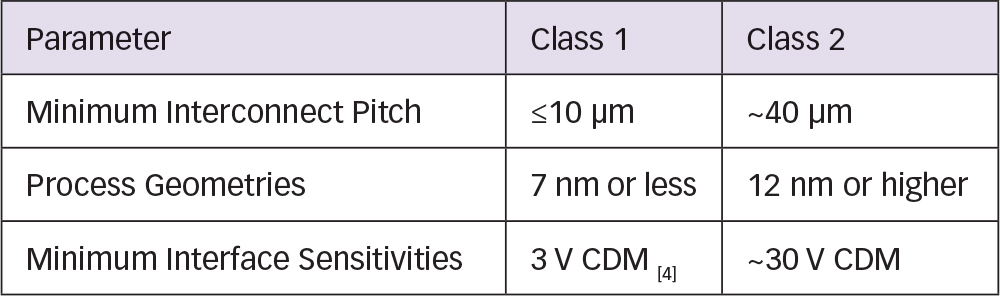
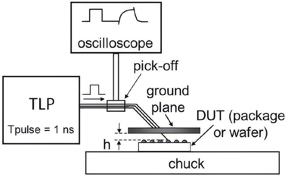
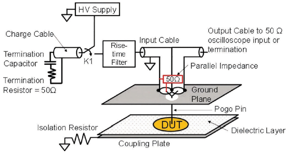
Let’s first focus on Class 2 chiplets. Class 2 chiplets, which currently have a minimum pitch of around 40 µm (with trends toward as low as 25 µm), while challenging to characterize with current test methods, can be addressed. The advantage of a Class 2 chiplet is that it can still be mechanically probed. However, as noted in [1], the current industry-accepted field-induced CDM (FICDM) test method cannot be used for CDM testing because the air discharge method is not repeatable at 30 volts, and the current commercial FICDM test systems would have significant difficulty probing a Class 2 microbump. The two most promising contact‑based CDM test methods are the capacitively‑coupled transmission line pulse (CC-TLP) and low impedance contact CDM (LI-CCDM), see Figures 1 and 2.
While characterizing Class 2 chiplets is challenging, addressing Class 1 chiplets brings on even more challenges, some of which are currently not possible with any existing test method. Today, even the contact‑first test methods discussed cannot probe a hybrid bond with pitches that are ≤ 10 µm. Solutions being considered vary. One option is to use sacrificial metal layers to allow probing access to some of these tight‑pitched interfaces for representative testing using contact‑first CDM test methods either at the wafer level or by packaging in a test vehicle. A second option is to rely much more heavily on electronic design automation (EDA) tools to verify the design. This is a “correct‑by‑design” approach that relies heavily on the accuracy of the automated tools and the manufacturing ESD controls in place to address the ESD risks.
Together, these two paths mark where the industry currently stands: contact-based CDM methods offer a workable, if still developing, route for Class 2 chiplets, while Class 1 chiplets continue to push past the limits of existing test and verification techniques. Part 2 of this series will take on the challenges that remain even after a test method is chosen, including correlation to FICDM, failure criteria, rise time, statistical sampling, and the demands placed on EDA verification tools.
- Kathleen Muhonen, “Small Form Factor CDM Testing, Part 1: Problems with FICDM Testing for Small Form Factor and Interface Die,” In Compliance Magazine, January 2026.
- Kathleen Muhonen, “Small Form Factor CDM Testing, Part 2: Air Discharge Options,” In Compliance Magazine, February 2026.
- Kathleen Muhonen, “Small Form Factor CDM Testing, Part 3: Contact First Methods,” In Compliance Magazine, April 2026.
- JEDEC JEP 196, “White Paper 2 Part II: Die-to-Die Interfaces,” Industry Council on ESD Target Levels, November 2023.
- ANSI/ESD SP5.3.4-2022 “Charged Device Model (CDM) Testing Component Level – Capacitively Coupled Transmission Line Pulsing (CC-TLP) as an Alternative CDM Characterization Method,” 2022.
- ANSI/ESD SP5.3.3-2018 “Charged Device Model (CDM) Testing – Component Level Low‑Impedance Contact CDM as an Alternative CDM Characterization Method,” 2018.