Future Challenges for System-Level HV ESD Protection and First-Time-Right Design

Editor’s Note: The paper on which this article is based was originally presented at the 43rd Annual EOS/ESD Symposium in October 2021. It was subsequently awarded the 2021 Symposium Outstanding Paper at the 44th Annual EOS/ESD Symposium in September 2022. It is reprinted here with the gracious permission of the EOS/ESD Association, Inc.
The automotive industry is experiencing a revolutionary transformation towards electrification, autonomous driving, as well as more connectivity and information. Thus, in-vehicle-network architecture is changing with an exploding amount of data cars need to process at high-speed. For example, infotainment content is rapidly increasing with an average of 20 cameras and 15 displays per vehicle. In addition, the new zonal architecture requires a new IP based protocol. Here, the automotive ethernet plays a key role for the links with data rates up to 1 Gbit/s today and multi-Gbit/s in the future. The so-called Open Alliance Committee defines a standard for those links in EHTERNET 100/1000BASE-T1, especially for the ESD protection device [1].
Figure 1 depicts the general trend (blue curve) of in-vehicle networks data-rates for different automotive protocols from the legacy LIN, CAN, FLEXRAY to the advanced protocols of ETHERNET up to SERDES. The orange curve shows the corresponding maximum of permissible parasitic capacitance of the discrete ESD component at the data line (partly from author’s experience).
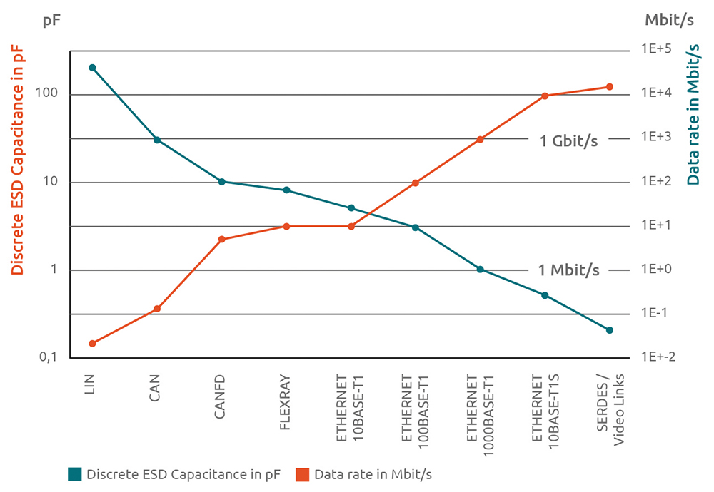
Significant ESD challenges result from the OPEN Alliance Ethernet specification [1], requiring the ESD protection device being robust for minimum of 1000 discharges at 15 kV ESD IEC 61000-4-2 pulse. At the same time, the discrete ESD capacitance is demanded to be continuously reduced for future high-speed protocols even below levels of 0.5 pF to ensure RF signal integrity. These two conflicting trends can only be met with highly advanced, discrete ESD architectures while on-chip ESD in the IC transceiver often does not suffice those requirements anymore.
In addition, the specification [1] recommends placing the external ESD component close to the connector, see Figure 3, instead of a position directly at the IC, i.e., behind the decoupling capacitors. The intention of this modification was to safeguard the overall system including all discrete components located in the signal path and to fulfill the EMC immunity requirements such as Direct Power Injection (DPI) acc. to IEC 62132-4 [2]. As a consequence of this placement, the new topology demands a more challenging high-voltage ESD specification with a high trigger Vt1 > 100 V and high holding voltage Vhold > 28 V to prevent triggering of the ESD protection device during normal operation and disturbances. For earlier Ethernet links, those high-voltage values were not required since a low-voltage discrete ESD component protection was sufficient behind the decoupling cap directly at the IC.
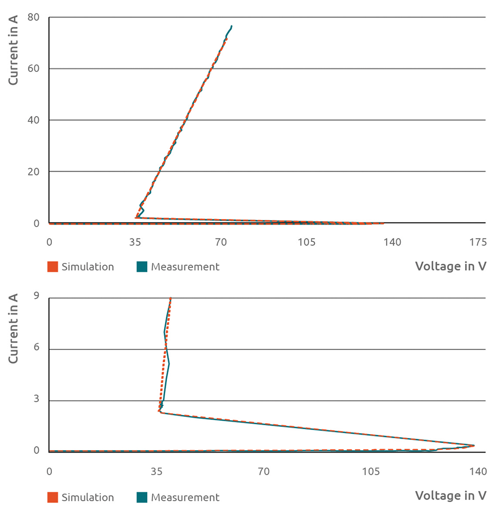
For those modern links described above, a silicon-based discrete ESD component (snapback-type) with Vt ≈ 140 V, Vhold ≈ 35 V, and Rdyn ≈ 0.1 Ω can be used, see Figure 2.


Figure 4 displays an example for a measured residual IC current transient IIC for 6 kV-ESD generator stress, acc. to [2], for two different protection device types, such as snapback and varistor, see TLP I-V characteristic in Figure 2. Apparently, the IC current can be safely limited applying the advanced snapback-type ESD protection device while the varistor admits an approximately 6x higher peak current into the IC due to the relatively high ESD voltage clamping.
This level violates even a 4 kV-HBM limit. It should be noted that the initial current spike demands a certain Charged Device Model (CDM) robustness-level from the transceiver IC for both cases, as discussed below in more detail. Apparently, limiting the systems ESD voltage exposure with appropriate discrete snapback clamps can be important for protecting advanced automotive high-speed interfaces.
Following system-level design challenges are addressed in this paper:
- CMC filters in the data-line play an important role also for ESD protection of the system IC as will be discussed in detail by measurement and simulation. Moreover, the CMC trend for smaller inductance L for higher data transmission may lead to a reduced ESD blocking capability of the CMC and this to a more critical ESD exposure to the entire system, as investigated by the transient SEED simulations Therefore, the ESD behavior of different CMCs is studied in detail and compared for the first time as well as its impact on system-level ESD protection.
- ESD discrete protection parameters become more challenging, since there is a trend towards an increased holding voltage, e.g., from 35 to 60 V or higher to comply for instance with a 48 V board nets and a robust system operation. This results in a larger ESD voltage stress for the system and thus higher currents into the RF-IO pins. In this paper, this behavior is investigated by system-level transient simulations based on the 1000BASE-T1 application.
A NoiseKen ESD generator was used for contact discharge of 1 kV into a 2 Ω Pellegrini target delivering a reference current waveform for model parameter extraction. Figure 5 shows a good fit between measurement and simulation [4].
![line graph illustrating current waveform of an ESD generator IEC 61000-4-2 [3] at 1 kV contact discharge through a 2 Ω reference target: simulation vs. measurement](https://digital.incompliancemag.com/asset/2023/08/incomp_sept2023-automotive_high-speed_interfaces-fig_05.jpg)
To predict both the dynamic (ref. first IEC current peak) and quasi-static (ref. second IEC current peak) system ESD performance, a precise behavioral model of the external ESD protection was created [4].
Figure 6 shows an excellent match of the quasi-static measured TLP I-V with the simulation.
As a result, the turn-on time caused by conductivity modulation of the high-resistive region creates a relatively large transient trigger voltage overshoot, see Figure 7. Consequently, for a high simulation accuracy an adequate modeling of this transient ESD behavior is crucial and demonstrated by a comparison to the corresponding simulation.


CMC operation during ESD
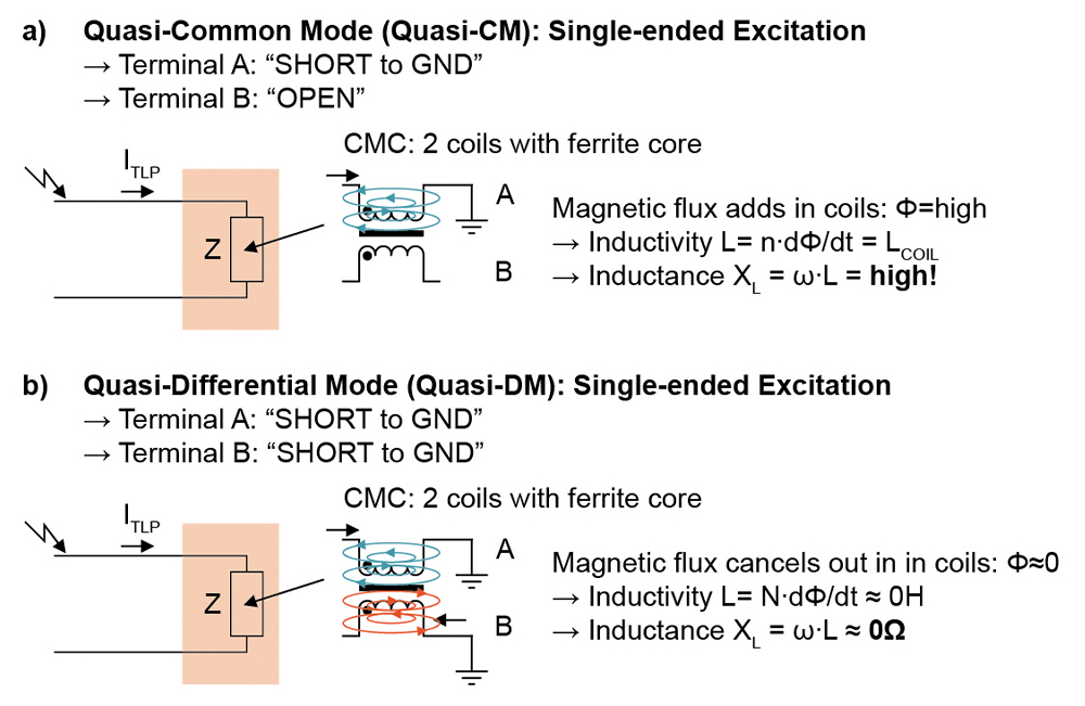
In the ESD stress case of one data line only, however, we can consider a third CMC operating mode. Here, the ESD pulse propagates only through one of the data-lines and thus coils, representing the so called “single-ended excitation” of the CMC, see Figure 9, with only one terminal being directly affected. To understand the behavior of the CMC in such an asymmetrical case of ESD disturbance, a TLP measurement method is applied as depicted in Figure 9.

Here rectangular pulses of different amplitudes and a constant pulse duration of 100 ns are injected into one of the two CMC terminals, while the remaining one will be kept in floating condition. A constant TLP rise time is set to be in the range between 600 ps and 1 ns which is very similar to the IEC61000-4-2 standard (see Figure 5) to ensure comparability.
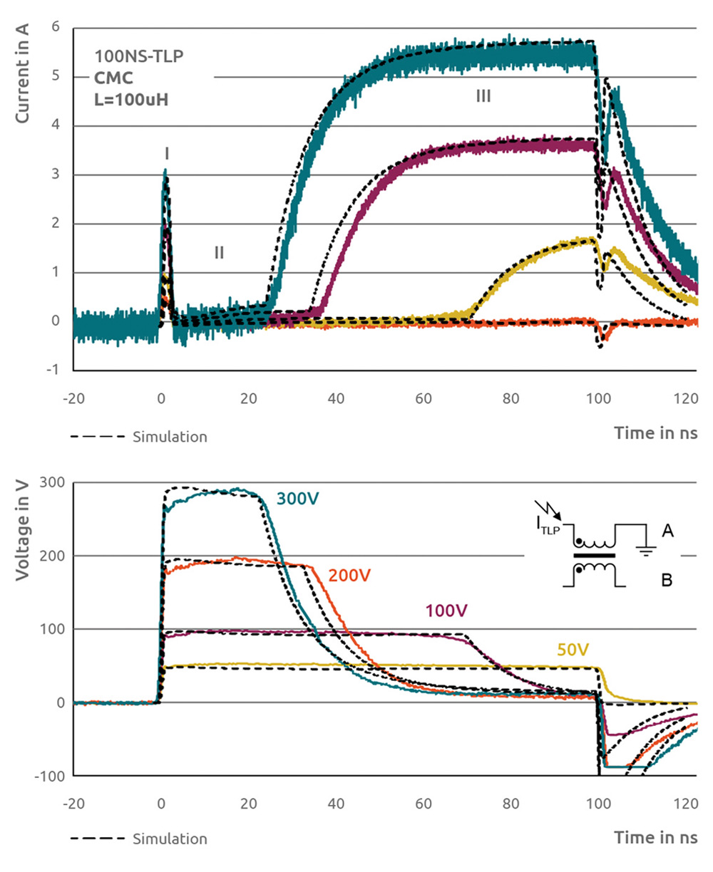
Figure 10 shows the resulting complex transient TLP current/voltage response of the CMC with L=100 µH in comparison to the corresponding simulation obtained with a CMC behavioral model (see dashed line), will be introduced later in this section.
Based on the transient curves, 3 characteristic regimes can be distinguished: dynamic (I) – voltage-dependent current overshoot in ns-range, a quasi-static regime of current blocking (II), and a current saturation (III). Those will be discussed in detail in the following.
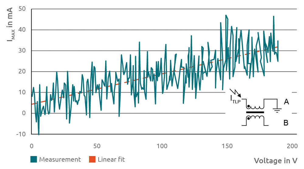
Since such an initial peak cannot be measured with standard 100 ns-TLP, vf-TLP was performed in the same single-ended excitation of terminal A with terminal B fully floating. Figure 11 shows the only small capacitive displacement current of up to 30 mA for a slew rate of about dV/dt ~ 200 V/ns at this operation point. Using I = C x dV/dt a coil capacitance of C = 150 fF can be estimated. This value is well in line with the 140 fF reported in [6] for high-impedance CM conditions only. Note that under DM operation the parasitic coupling coil capacitance increases significantly to C~10 pF. [6].
As mentioned above and discussed in Section III in our IEC system-level experiments, we can clearly observe an initial fast current peak of high amplitude similar to the 100 ns-TLP artefact. This peak is very relevant for IC system-level protection as well and far larger in the amplitude than the small current peak we would expect based on the results shown in Figure 11, where the standalone CMC operates in quasi-CM. So why do we observe such an assumed contradiction in CMC behavior when used in a system circuitry showing a first current peak related to a large DM capacitance, but a current blocking behavior related to a quasi-CM state? This question will be addressed in Section III.
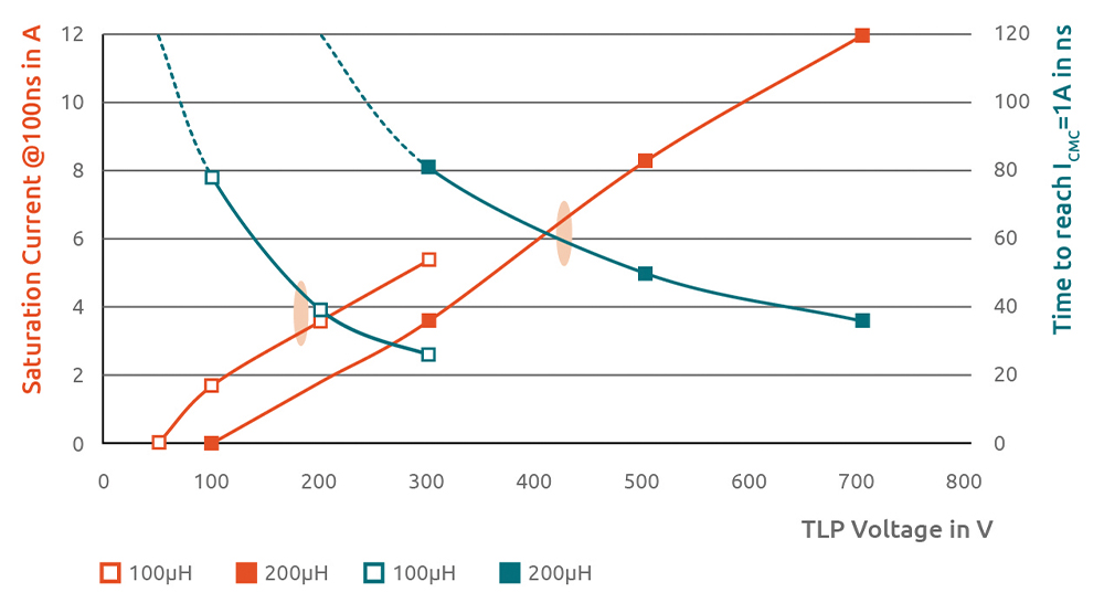
The onset of the CMC saturation is dependent on the voltage level across the excited CMC coil. The higher the voltage level, the earlier the magnetic saturation of the ferrite core occurs. Saturation leads to a significant increase of the current through the CMC, see Figure 10. In that case the current blocking capability of the CMC will be lost due to transition into low-impedance or ohmic state. This detrimental behavior of the CMC for ESD should be carefully considered during the design of the Ethernet system and the ESD protection circuitry. Here, transient SEED simulation with an appropriate CMC model is a powerful tool for first-time right design. In the following, a behavioral CMC model will be introduced. Based on the observations, the Quasi-CM behavior of the CMC will be used for model tuning.

To realize the resistance change of the signal path, a voltage dependent resistor (switch) is connected in parallel to the signal path of the CMC. To provide smooth transition from high- to low-impedance state and describe current rise and voltage decay over time properly, an inductor is connected in series to the voltage dependent resistor as well. In addition, to fine tune the voltage offset in the low-impedance state a DC voltage source can be placed in series with the switch and inductor. Finally, to control the voltage change at the switch a control unit circuitry represented by an RC network and extended by a feedback loop are implemented. The latter is required to keep the reached control voltage levels for the switch during the whole saturation regime constant.
In the next chapter a system-level ESD analysis and risk assessment for multi-Gbit configuration will be performed taking into account the changed CMC ESD blocking characteristic due to more challenging SI requirements of the high-speed data links.
For system-level measurements and SEED simulations Ethernet emulation network based on the specification [1] is used, see Figure 15. The decoupling capacitors of 100 nF are practically transparent for ESD pulses due to the very high dynamics of the ESD generator and, hence, do not impact the ESD behavior significantly. The CMT though seems to have an impact on the conduction state of the CMC as discussed below. The transceiver IC is emulated in a simplified but fairly critical way using a resistor network of 2-Ohm according to the OPEN Alliance specification [1].
![diagram of thernet ESD current test circuitry including standardized IC emulation network formed by resistors [1]](https://digital.incompliancemag.com/asset/2023/08/incomp_sept2023-automotive_high-speed_interfaces-fig_15.jpg)
![line graph illustrating 4 kV ESD generator system-level measurement vs. simulation with snapback ESD device and a CMC L=200 µH [4]](https://digital.incompliancemag.com/asset/2023/08/incomp_sept2023-automotive_high-speed_interfaces-fig_16.jpg)
- Coil B is not fully floating but connected to the IC I/O with its internal ESD protection circuitry as emulated by the 2 Ohm resistor, same as coil at terminal A
- A CMT network is connected to the CMC terminals at D+/D- thru the dc block (which can be neglected in the ESD time domain due to capacitance value)
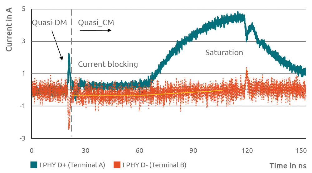
The green curve represents the quasi-CM which was already introduced as a high-impedance state with transition into low impedance saturation. As opposed to this behavior, the red curve demonstrates the response of the CMC where terminal B is shorted to GND same as terminal A instead of floating.
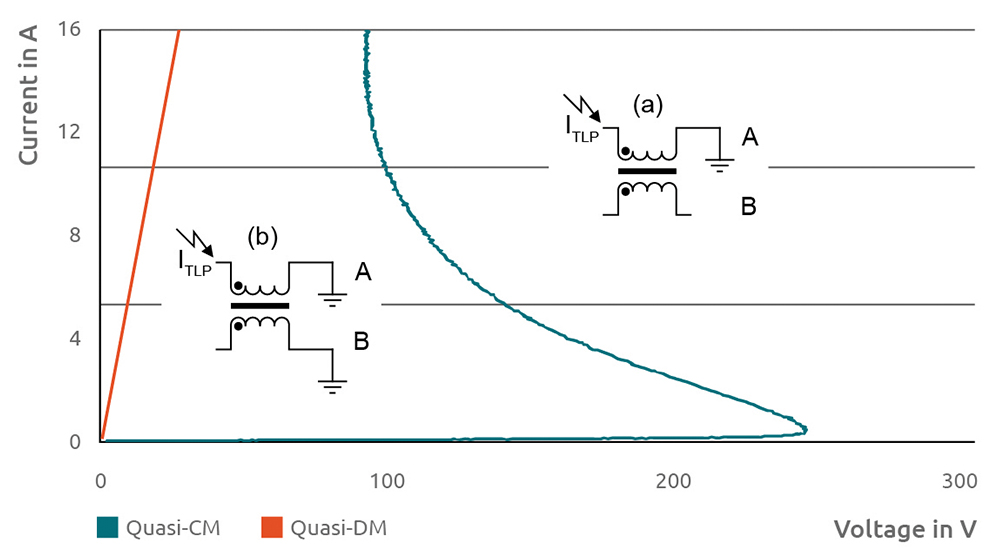
The result for quasi-DM condition contradicts the fact that we observe only a small residual current flowing into the IC, see Figure 16. That means, that CMC, being used in Ethernet circuitry acts in a high-impedance blocking state, as could be explained by quasi-CM, allowing the external ESD protection component to turn on and finally protect the IC.
Based on additional transient measurement on system-level, we developed a hypothesis to resolve this contradictory issue. Here, we considered the full board circuitry including the CMT network as a discriminating factor compared to our standalone CMC analysis. Figure 19 shows TLP time domain curves, where the CMT network including decaps is connected to the CMC from the left side and a 2 Ohm resistor terminates each of the CMC channels from the other side.
Here, no external ESD protection was connected between D+/D- and ground. Based on the results, we can conclude that a mix of two different operating modes occur for the CMC. At the onset of the pulse, during the first nanoseconds, the CMT is transparent and negligible for the entering TLP pulse. This is due to the fact the 1k-resistors are inflicted by parasitic inductance of several nH. Thus, the CMT circuit is an open which leads to a floating input of coil B. As shown in section III. A, this quasi-DM state has a low impedance and a high capacitance across the coil in the order of ~10 pF.
However, after some time the CMT network starts to shift the current phase between Terminals A and B of the CMC thus preventing the magnetic flux cancelation. As a result, the CMC transits into the high-impedance quasi-CM condition. Due to a relatively large time constant of the CMT τ = R x C ~ 5 µs, the charging of the CMT capacitance should last during the entire ESD event keeping the CMC in the quasi-CM until saturation. In blocking mode, the CMC can strongly support the external ESD protection consequently avoiding any significant residual current into the IC during the entire ESD pulse, see Figure 19. In case the applied TLP voltage level is high enough, also the onset of saturation within quasi-CM regime can be observed.
For a system-level ESD protection it is obvious, that CMC alone is not capable to suppress the current initiated by the single-ended injection of ESD pulse and needs to be extended by an appropriate CMT network. In the full system circuitry, the CMC, CMT and the external ESD device are building a synergy significantly extending the entire system ESD robustness. On the one hand, the blocking characteristic of the CMC during the first nanoseconds helps to trigger the ESD protection device. On the other hand, the ESD device takes the majority of the ESD current protecting consequently not only the IC, but rather the entire circuitry incl. CMC and CMT. A more detailed explanation based on a SEED simulation is given in the next subsection.
Firstly, a discrete ESD device with snapback and a larger holding voltage Vhold of 60 V is considered due to the trend to higher battery voltages for hybrids and electrical vehicles. Secondly, a CMC with reduced inductance L of 100 µH is used due to higher data rates, hence, less inductance and parasitics will be added to the D+/D- in the context of signal integrity [1]. Figure 20 depicts the results of the transient simulation for this example for 4 kV-IEC system-level stress.
As can be seen in Figure 20 (green curve), the non-linear behavior of the CMC in conjunction with the ESD protection device turn-on behavior and clamping dynamics creates a critical current profile thru the sensitive IC I/O. Due to increased ESD clamping voltage (larger Vhold) and the lowered CMC blocking capability (smaller L), the current into the IC I/O connected to the D+ data-line, would slightly exceed in its peak value at 60 to 70 ns a 4 kV-HBM IC robustness level.

After a duration of approximately 40 ns, the CMC enters saturation, thus gradually losing its blocking capability. As a result, the current into the IC interface at D+ increases (green curve). Due to this competitive conduction with the CMC, the ESD device eventually starts to turn off at 60 ns, as soon as current and voltage levels at the ESD protection get too low to keep it further on. At this time, the CMC also reaches saturation (i.e., lowest impedance) while the current into the IC attains its maximum. This peak current slightly exceeds the 4 kV-HBM limit.
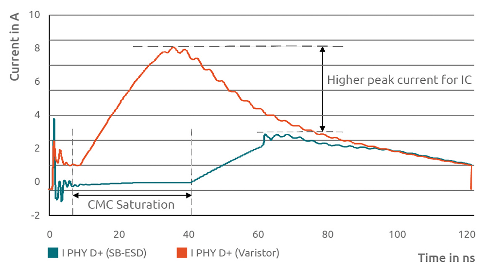
This simulation example clearly demonstrates the important synergetic protection mechanism of the ensemble of CMC and ESD within a complex system circuitry. Important to note in this context is that an enhanced ESD voltage clamping limits the residual IC current by two effects: a) the more trivial lower voltage exposure to the IC, b) the subtle effect of keeping the CMC for a longer duration in a current blocking mode before reaching low-impedance saturation.
The latter effect is highlighted by system-level simulation with a varistor in comparison to the snapback ESD protection in Figure 21. The higher clamping voltage of the varistor obviously provokes a much earlier onset of CMC saturation at about 10 ns instead of 40 ns observed for the more effective snapback clamp. As a result, the current into the IC (PHY) reaches an almost three times higher peak value compared to the snapback protection as well as a significantly longer stress duration almost during the entire energetic part of the IEC pulse. Thus, the overall IC stress energy and risk of failure significantly increases.
For the SEED simulations on system-level described in the paper, the complex high-current CMC characteristic was incorporated into a non-linear behavioral CMC model. Applying both CMC and ESD non-linear dynamic behavioral models, the system simulation results clearly illustrate the synergy effects of CMC and the discrete ESD protection as also confirmed by appropriate measurements (TLP, IEC 61000-4-2). As major finding, it turned out that a lower ESD clamping voltage enabled by a well-tuned, high-voltage snapback device offers a superior protection not only due to the trivial effect of less voltage exposure to the IC. Another strong second benefit is that the lower ESD voltage exposed to the CMC keeps the inductance for a longer duration in a blocking state. Thus, the IC is perfectly shielded from the ESD until the CMC enters the low-resistive saturation mode. Such a prolonged blocking time can be sufficient to keep out the high-current, high-energy IEC peaks in conjunction with a well-designed ESD component.
The paper highlights the benefit of a SEED simulation-based pre-design phase of the more advanced automotive high-speed links. Moreover, the tool allows an appropriate selection of external ESD and passive components to achieve a first-time right system ESD design in compliance with RF signal integrity.
References
- OPEN Alliance, “IEEE 1000BASE-T1 EMC Test Specification for ESD Devices,” Version 1.0, date 27.10.2017.
- IEC 62132-4, “Integrated circuits – Measurement of electromagnetic immunity – Part 1: General conditions and definitions,” Edition 2.0, 2015.
- IEC 61000-4-2, Edition. 2.0 Standard, ESD Immunity Test, 2008.
- Sergej Bub et al. “Efficient prediction of ESD discharge current according to OPEN Alliance 100BASE-T1 spec using SEED,” ESD Forum, Germany, 2019.
- M. Ammer et al, “Characterization and Modeling Common Mode Inductors at High Current Levels for System ESD Simulations,” EOS ESD Symposium, 2019.
- S. Mortazavi, “Characterization of Common-Mode Choke for Automotive Ethernet Networking enabling 100 Mbit/s,” Proceeding of International Symposium on Electromagnetic Compatibility, September 2017.
- N. K. Kranthi et al. “Insights into the System-Level IEC ESD Failure in High Voltage DeNMOS-SCR for Automotive Applications,” 2020 42nd Annual EOS/ESD Symposium (EOS/ESD), 2020, pp. 1–7.
- “How to Use Picoprobes and Flexible Pitch Probes,” 2021. https://www.hppi.de/files/AN-010.pdf
