EMC concepts explained
Return-Current Distribution in a PCB Microstrip Line Configuration
Part 2: Reference Plane with Discontinuities
T

his is the second article of a two-article series devoted to the return current distribution in a PCB microstrip line configuration. The previous article [1] presented the CST simulation results in the case of a solid reference plane. This article addresses the case where the reference plane contains several discontinuities: edge slot, internal slot, slot holes, and via cutouts.

1. Baseline Results
In [1], we presented the baseline results for a solid reference plane and showed the return current path (forward current trace is hidden) flowing in the reference plane at different frequencies.

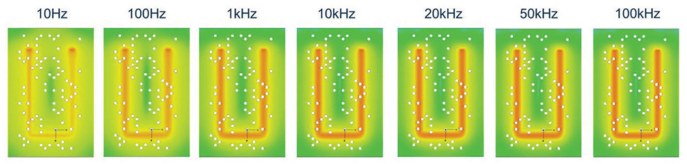
The results showed that at 10 Hz the return current spreads wide over the reference plane, flowing both under the top trace and directly from the load port to the source port. As the frequency increases to 100 Hz, more of the return current flows under the trace (with a narrower spread), and less of it flows directly from the load port to the source port. This trend continues as the frequency increases to 1 kHz. As the frequency increases beyond 10kHz, the return current path remains virtually unchanged, predominantly flowing beneath the forward trace. In other words, the return current path and current density no longer depend on frequency.

Figure 1: CST Model – Two-layer PCB with an edge slot in the reference return plane
Figure 1: CST Model – Two-layer PCB with an edge slot in the reference return plane
The results were confirmed by plotting the normalized current distributions.
2. PCB with Edge Slot
Figure 1 shows the CST Studio model of a two-layer PCB with an edge slot in the reference plane.

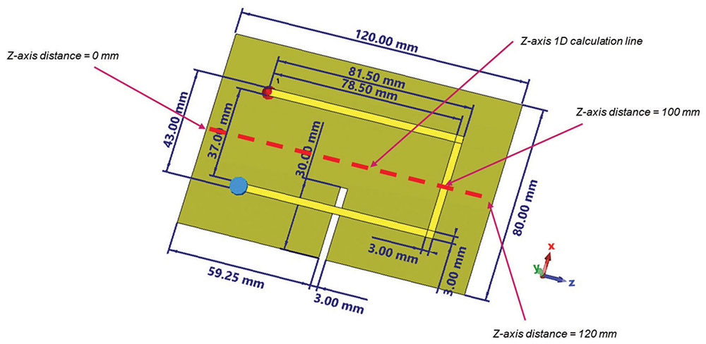
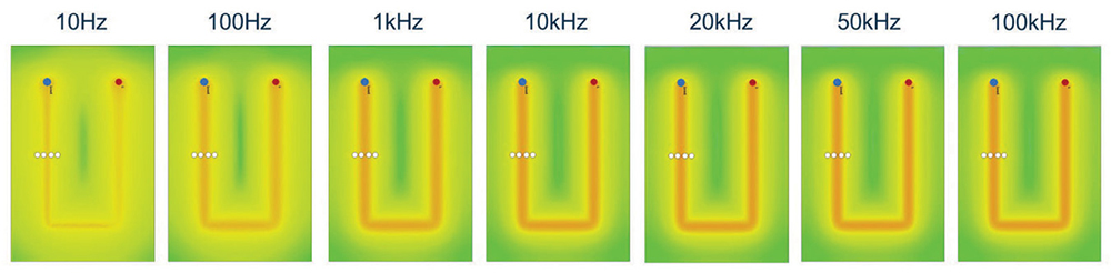
Figure 2 shows the return current path (forward current trace is hidden) flowing in the reference plane at different frequencies.

The results show that the edge slot forces current to go around it and flow in a larger loop (higher inductance). The return current exhibits the frequency-dependent behavior similar to the solid reference plane case.

Figure 2: Edge slot - return current path at different frequencies
Figure 2: Edge slot – return current path at different frequencies
At lower frequencies (below 1 kHz), the return current spreads wide over the reference plane, flowing both under the top trace and directly from the load port to the source port. This trend continues as the frequency increases to 1 kHz. As the frequency increases beyond 10 kHz, the return current path remains virtually unchanged, predominantly flowing beneath the forward trace, the return current path and current density no longer depend on frequency.

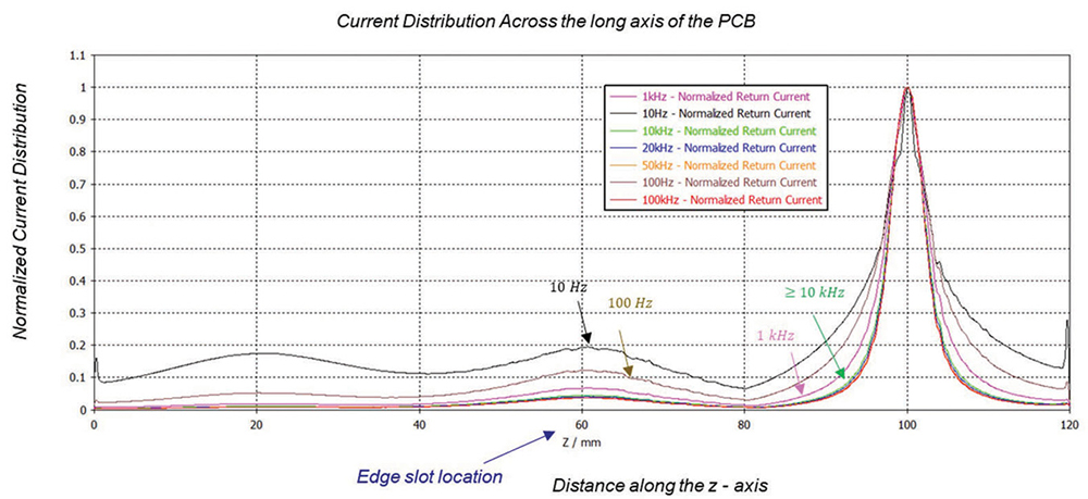
This is confirmed by the normalized current distributions shown in Figure 3.

Figure 3: Edge slot - normalized current distributions at different frequencies
Figure 3: Edge slot – normalized current distributions at different frequencies
3. PCB with Internal Slot
Figure 4 shows the CST Studio model of a two-layer PCB with an internal slot in the reference plane.
Figure 4: Internal slot in the reference return plane – CST model
Figure 4: Internal slot in the reference return plane – CST model
Figure 5 shows the return current path flowing in the reference plane at different frequencies.
Figure 5: Internal slot - return current path at different frequencies
Figure 5: Internal slot – return current path at different frequencies
The results show that current returns around both sides of the slot and thus does not ‘bulge’ as much as the edge slot case. The return current exhibits the frequency-dependent behavior similar to the edge slot and the solid reference pane case. As the frequency increases beyond 10 kHz, the return current path remains virtually unchanged, predominantly flowing beneath the forward trace, the return current path and current density no longer depend on frequency.

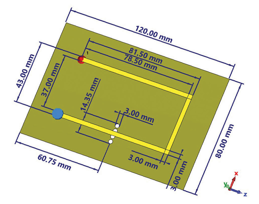
This is confirmed by the normalized current distributions shown in Figure 6.

Figure 6: Internal slot - normalized current distributions at different frequencies
Figure 6: Internal slot – normalized current distributions at different frequencies
4. PCB with Slot Holes
Figure 7 shows the CST Studio model of a two-layer PCB with slot holes in the reference plane.
Figure 7: Slot holes in the reference return plane – CST model
Figure 7: Slot holes in the reference return plane – CST model
Figure 8 shows the return current path flowing in the reference plane at different frequencies.

The impact of the holes is minimal compared to the solid reference plane case. Return currents are permitted to flow between and around the holes and therefore the current does not bulge away from the return path out toward the middle of the PCB. The results are very similar to the previous cases: as the frequency increases beyond 10 kHz, the return current path remains virtually unchanged, predominantly flowing beneath the forward trace, the return current path and current density no longer depend on frequency.

Figure 8: Slot holes - return current path at different frequencies
Figure 8: Slot holes – return current path at different frequencies
This is confirmed by the normalized current distributions shown in Figure 9.
Figure 9: Slot holes - normalized current distributions at different frequencies
Figure 9: Slot holes – normalized current distributions at different frequencies
5. Ground Via Cutouts
Finally, we investigate the PCB with several ground via cutouts. Figure 10 shows the CST Studio model.
Figure 10: Two-sided PCB with via cutouts in the reference plane
Figure 10: Two-sided PCB with via cutouts in the reference plane
Figure 11 shows the return current path on the reference plane at different frequencies.
Figure 11: Ground via cutouts - return current path at different frequencies
Figure 11: Ground via cutouts – return current path at different frequencies
The results are similar to the previous cases and are confirmed by the normalized current distributions at different frequencies, shown in Figure 12.
Figure 12: Ground via cutouts - normalized current distributions at different frequencies
Figure 12: Ground via cutouts – normalized current distributions at different frequencies
Conclusions
Ground plane discontinuities do affect the return current path to various degrees by increasing the loop area, and thus increasing the inductance. In all cases, however, the return current exhibits very similar frequency-dependent behavior. As the frequency increases beyond 10 kHz, the return current remains virtually independent of increasing frequency.
Reference
  1. Bogdan Adamczyk and Scott Mee, “PCB Return-Current Distribution in a PCB Microstrip Line Configuration, Part 1: Solid Reference Plane,” In Compliance Magazine, August 2023.
Share this story:
Bogdan Adamczyk headshot
Dr. Bogdan Adamczyk is professor and director of the EMC Center at Grand Valley State University (http://www.gvsu.edu/emccenter) where he regularly teaches EMC certificate courses for industry. He is an iNARTE certified EMC Master Design Engineer. Prof. Adamczyk is the author of the textbook “Foundations of Electromagnetic Compatibility with Practical Applications” (Wiley, 2017) and the upcoming textbook “Principles of Electromagnetic Compatibility with Laboratory Exercises” (Wiley 2023). He can be reached at adamczyb@gvsu.edu.
Bogdan Adamczyk headshot
Scott Mee is a co-founder and owner at E3 Compliance which specializes in EMC & SIPI design, simulation, pre-compliance testing and diagnostics. He has published and presented numerous articles and papers on EMC. He is an iNARTE certified EMC Engineer and Master EMC Design Engineer. Scott participates in the industrial collaboration with GVSU at the EMC Center.