Existing methods of CDM simulation do not reliably predict the failure level of circuits with thin GOX gate at the pad. It was shown in [2] that for the GOX directly at pad the failure is caused by the initial fast current step of 20ps or less of the CDM event. It was also shown that the inductance of the critical path is very important for CDM performance. In another study [7], Charged Coupled (CC)-TLP, with pulse risetime of 20ps, has been demonstrated to predict CDM robustness reliably.
In this work, CDM simulation approach with stimulus current having initial risetime component of 20ps is investigated. The analysis is supported by CDM measurements of packaged Low Noise Amplifier (LNA) circuits, Very Fast (VF)-TLP measurements with 100ps risetime and ultrafast TLP (UF-TLP) measurements with 20ps risetime. To achieve a fast and simple simulation method the simulation is restricted to the receiver circuit itself and the complex RC network of charge distribution across the chip usual for CDM simulations are neglected and a simple charge distribution between VSS and VDD rail is assumed [3]. This is a valid assumption for designs using a common VSS rail for the IP block under investigation. Interconnect and device parasitics are considered by introducing parasitic resistance and inductance values to the schematic for CDM SPICE simulation. Resistance values are extracted. The initial range of inductance values are gained from layout assessment, which is refined based on the voltage measurements at the pads of reference structures. Capacitive coupling between metal lines is accessed to in range of femto-farad, the effects are considered negligible. The simulation is valuable both for an early design study with preliminary target values for resistance and inductance and for the final design using extracted values from layout. An excellent agreement of simulated and measured CDM failure thresholds for CDM currents could be proven for a large set of LNA test structures.


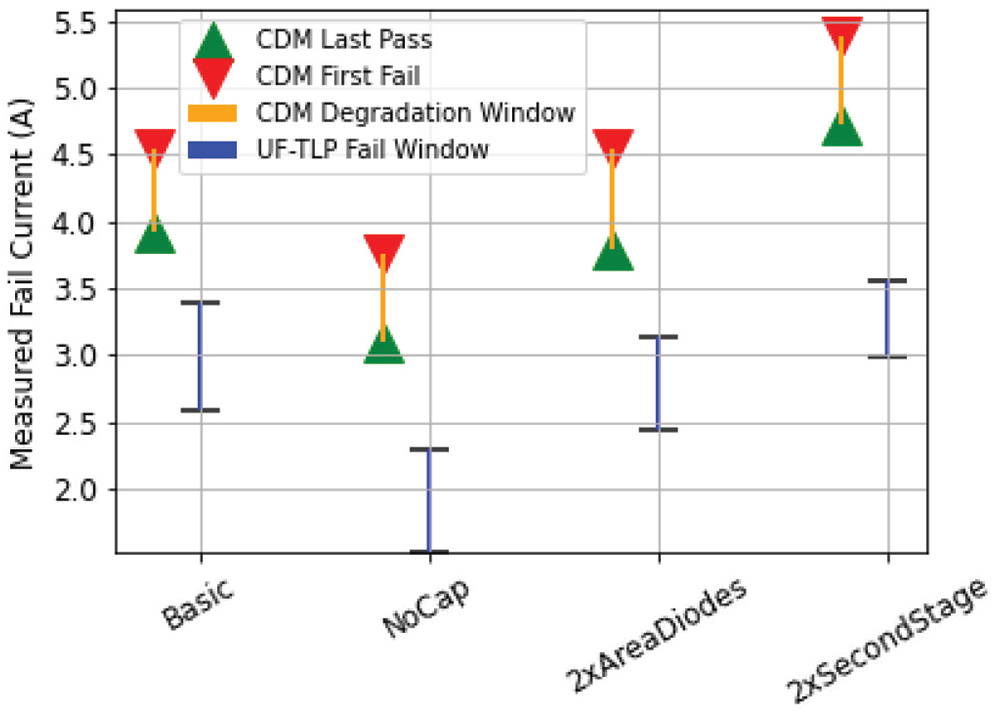
During a CDM event the sensitive gate oxide connected to the pad in an LNA circuit is damaged by the fast rise time component of 20ps or less as shown in [2]. VF-TLP with 1ns pulse width and 100ps rise time shows no correlation with CDM test (shown in Figure 2) and thus, cannot be used for predicting CDM robustness. Contrary to the expectation raised from the overestimation of the single LNA in [2], the CDM robustness can also be underestimated or show a “lucky” fit with the VF‑TLP results, depending on the circuit.


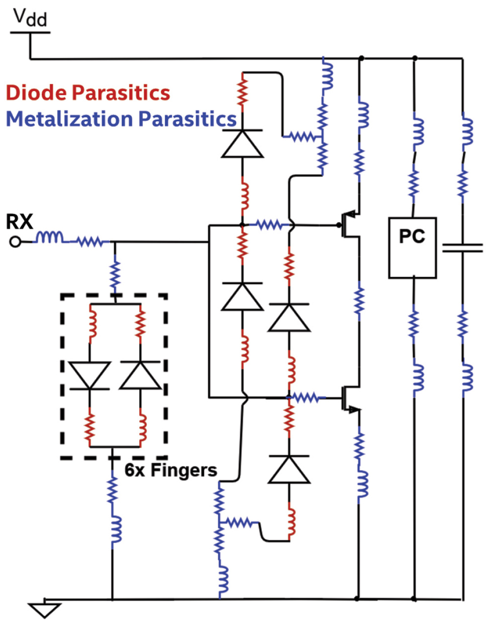

The VSS network is relatively large, in terms of area, compared to the VDD network in our test structures. Considering the ratio, we assumed distribution of CDM relevant change of 10% on the VDD network and 90% of the charge on the VSS network. The CDM charge sources are simulated as current sources where the current source between pad and VSS rail contributes 90% of the current and the second current source between pad and supply rail adds 10% to the CDM current at the pad. The current waveform, shown in Figure 9, is used as current force into RX during transient analysis of circuit, as shown in Figure 6, in SPICE simulation. The maximum voltage across GOX of the victim from the voltage pulse in Figure 10, is compared it to the oxide breakdown voltage as the failure criteria.


- P. Tamminen, R. Fung, and R. Wong, “Charged device ESD threats with high-speed RF interfaces,” 2017 39th Electrical Overstress/Electrostatic Discharge Symposium (EOS/ESD), pp. 1-8, 2017.
- D. Johnsson, K. Domanski, and H. Gossner, “Device Failure from the Initial Current Step of a CDM Discharge,” in Electrical Overstress/Electrostatic Discharge Symposium (EOS/ESD), Reno, 2018.
- S. S. Poon, K. Sreedhar, C. Joshi, and M. Escalante, “A Full‑Chip ESD Simulation Flow,” in Electrical Overstress/Electrostatic Discharge Symposium (EOS/ESD), Reno, 2015.
- A. Jahanzeb Y-Y. Lin, S. Marum, J. Schichl, and C. Duvvury, “CDM Peak Current Variations and Impact upon CDM Performance Thresholds,” Proc. EOS/ESD Symposium, pp. 283-288, 2007.
- Ansys Pathfinder. https://www.ansys.com/products/semiconductors/ansys-pathfinder-sc
- J. Willemen et al., “Characterization and Modeling of Transient Device Behavior under CDM ESD Stress,” Electrical Overstress/Electrostatic Discharge Symposium, Las Vegas, 2003.
- J. Weber, R. Fung, R. Wong, H. Wolf, A. Horst Gieser, and L. Maurer, “Comparison of CDM and CC-TLP robustness for an ultra-high speed interface IC,” 2018 40th Electrical Overstress/Electrostatic Discharge Symposium (EOS/ESD), pp. 1-9, 2018.
- C. Russ et al., “Enablement, Evaluation and Extension of a CDM ESD Verification Tool for IC Level,” 43rd Annual EOS/ESD Symposium (EOS/ESD), 2021.