

Close-up of a bright, branching electrostatic discharge (ESD) spark emitting from the tip of a metal probe against a blurred background.
Basing CDM ESD Test Goals on Fundamental Limits
Knowing Worst-Case Limits Helps Set CDM Test Goals Based on Use Conditions
W

hen we mention the charged device model (CDM) in electrostatic discharge (ESD), we could be referring to the essential factory event (referred to in this text as ChDE, or charged device event), or to the simulated event in a CDM tester, JS-002 in particular (see Reference 1).

A recent publication (Reference 2) used radial transmission line (RTL) theory to formulate the most accurate analytical model yet for these two versions of CDM, whereby a charged circular plate discharges at its center into a ground plate, as shown in Figure 1. RTL theory captures the essentials of both CDM cases and applies best to the real-world or actual use condition ChDE, again in Figure 1, representing component handling and die attach operations almost perfectly.
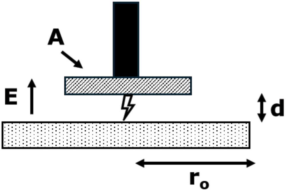
Figure 1: Typical CDM event configuration. We model a device of area A as being an equivalent circular disk above a ground plane.
Figure 1: Typical CDM event configuration. We model a device of area A as being an equivalent circular disk above a ground plane.
In this article, we will use the basic results of RTL theory to find out how severe CDM events (i.e., ChDE) might be for devices of a given size. This will help address what our true CDM test expectations for the devices should be, as there is very little guidance on how much CDM performance is “good” or “enough,” based on use conditions and device dimensions. Particularly with the introduction of more reproducible, spark-free, contact-first, CDM-like tests, we will want to specify criteria, such as peak current Ipk, along with rise time and slew rate (A/nsec of rising current edge), that would be acceptable as a CDM test for a given device, irrespective of the exact method used.

Many years of failure analysis after CDM testing, and correlation with factory failures, have convinced us that Ipk is the strongest indicator of a failure threshold from the measured waveform, as long as charge Q in the main pulse flows within a time scale (nanosecond or sub‑nanosecond) appropriate to the device size. Beyond that, rise times and slew rates are sometimes cited in reference to oxide failures because of the sharp rising edge of the pulse.

It therefore makes sense to have some minimum expectations, probably for slew rate rather than rise time. Like Ipk, slew rate scales with Q or surface electric field E, while minimum rise time is more a measure of the wave propagation time across the device, so small devices have fast rise time, due to reflection from the boundary. Slew rate depends only weakly on device size and scales with Q or E.

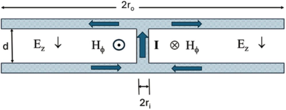
As described in Reference 2 and pictured in Figure 2, the RTL model has only vertical E-field Ez and axial H-field Hφ, with no fringing fields. This results in a simple but effective first approximation of capacitance:

Equation 1
and inductance
Equation 2
where ri is the inner disk radius (probe or spark channel), ro the outer radius, and d the plate separation. Equation 1 is the familiar parallel-plate capacitance formula, where we use other resources to estimate the equivalent outer radius ro due to fringing fields and possible non-circular geometry. Equation 2 is a simple model of inductance, not usually seen in CDM work until discussed in Reference 2, based on boundary conditions for current at the inner radius (conducting probe or spark channel) and at the plate boundaries. It is fairly accurate for d << ro, exactly what we expect for component handling or die attach.
Figure 2: Side view of RTL current flow and field pattern for open circuit at periphery (outward wave vectors). The current flows through the spark channel in the middle for events such as in Figure 1.
Figure 2: Side view of RTL current flow and field pattern for open circuit at periphery (outward wave vectors). The current flows through the spark channel in the middle for events such as in Figure 1.
In this article, the spark channel ri will be presumed to be no larger than 10 μm (it is usually smaller) and a negligible influence on die or component capacitance.

In the RTL model, the LC product, and thus ω0, is insensitive to the plate separation d, as also seen in the product of Equations 1 and 2. This property is important and leads us into our subject here, worst-case considerations of the factory ChDE

We start with the basic 2-pole underdamped decaying exponential solution for peak current, developed for a 2014 paper (see Reference 3) in these terms:

Equation 3
C is capacitance, V0 is voltage (thus Q = CV0), L is inductance, and D is damping factor RC/(2√LC) or RCw0/2. Ipk is highest for D = 0, so Ipk can be no higher than Qω0, rise time no faster than 1/w0, and slew rate (A/nsec of rising current edge) no faster than Qw02. These are the fundamental limits that we will use as we work toward arriving at reasonable CDM performance expectations for devices of a certain size, under expected use conditions.

At this point, we’re nearly ready to calculate Ipk and other limits as a function of effective outer radius and fundamental constants relating to wave propagation. Equations 1-3 give us an estimate of worst-case w0 = 1/√LC, leaving only charge Q to determine the important parameters (Ipk= Qw0, slew rate = Qw02) for a given size, i.e., equivalent radius r0.

The results presented in Reference 2 show that, after solving the RTL problem with circular Bessel functions, the estimates from Equations 1-3 need only a slight adjustment for parameter α in the following:

Equation 4
where τ0 = r0/c, c the speed of light. While Equations 1 and 2 would give α = √2/2=0.707…, the detailed RTL solution and analysis in Reference 2 find that 0.6433 < a < 0.7064, so our worst case is with α=0.6433. This fixes the scaling for Ipk, rise time (= 1/w0, the 1 radian time being the 10-90% rise time for a sinusoid), and slew rate. Now we turn to charge Q to complete the calculation.

Under use conditions (ChDE), the charge Q caused by CDM events could be due to tribocharging or to external fields from charged surfaces, resulting in induced charge on the component or die. In either case, field meters are employed in the factory to keep CDM events under control, so the goal is to keep E-fields below some achievable value. Here, we will use E = 100 V/cm as a goal and show that Q scales linearly with field. As Gauss’s Law relates surface charge density σ to perpendicular field through σ = ε0E, we find that:

Equation 5
thus worst-case
Equation 6
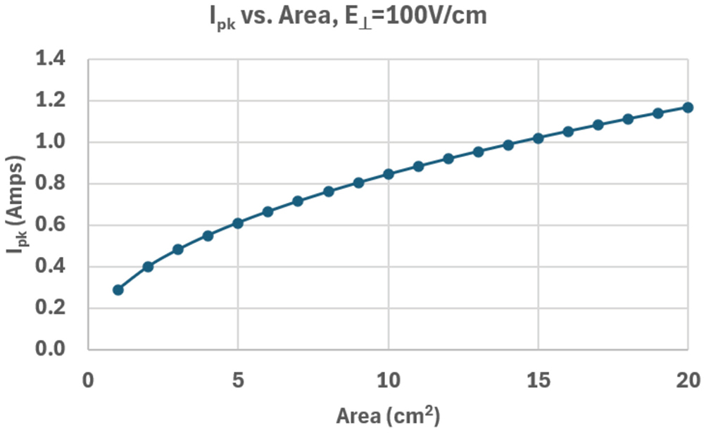
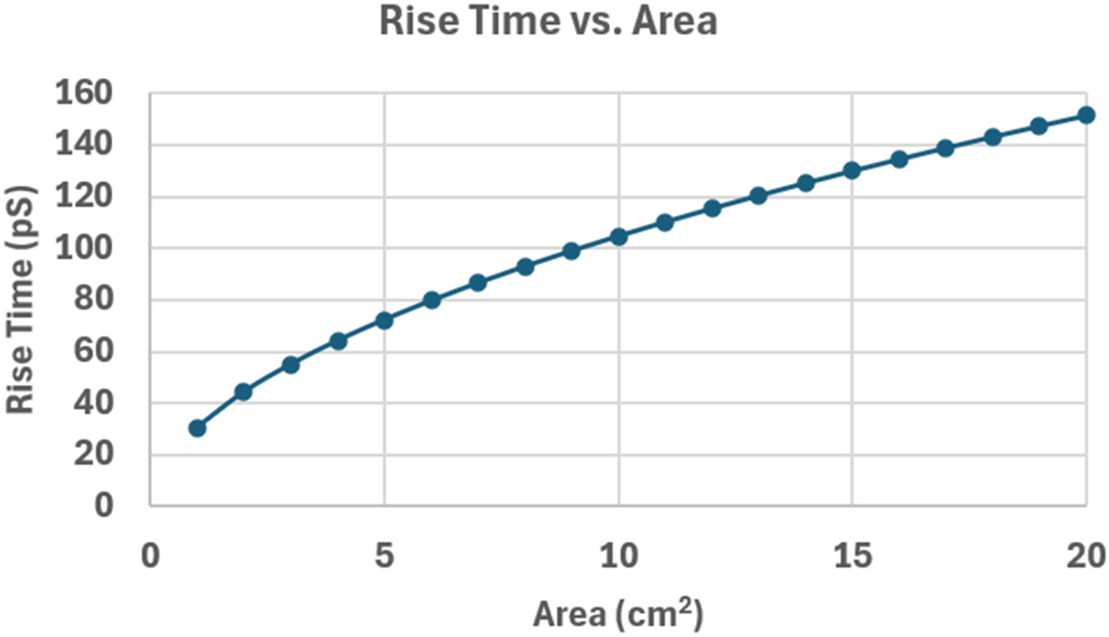
when we put in the lowest value of α. This Ipk limit is plotted in Figure 3 for E = 100V/cm, while minimum rise time ≥ 1/ω0, from Equation 4, appears in Figure 4.
Figure 3: Worst-case peak current vs. area (pr02); scales linearly with electric field E⊥
Figure 3: Worst-case peak current vs. area (πr02); scales linearly with electric field E
Figure 4: Minimum rise time vs. area, for a spark channel of radius ri = 10 µm
Figure 4: Minimum rise time vs. area, for a spark channel of radius ri = 10 µm
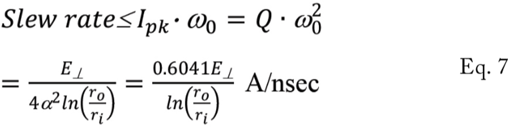
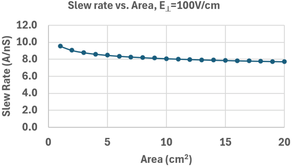
Both are plotted in terms of equivalent area A=πr02, corresponding to the die or package size. The slew rate limit, nearly independent of A, is:
Equation 7
again plotted vs. A and with E =100V/cm, in Figure 5.
Figure 5: Worst-case slew rate; scales with E⊥ with weak dependence on area
Figure 5: Worst-case slew rate; scales with E with weak dependence on area
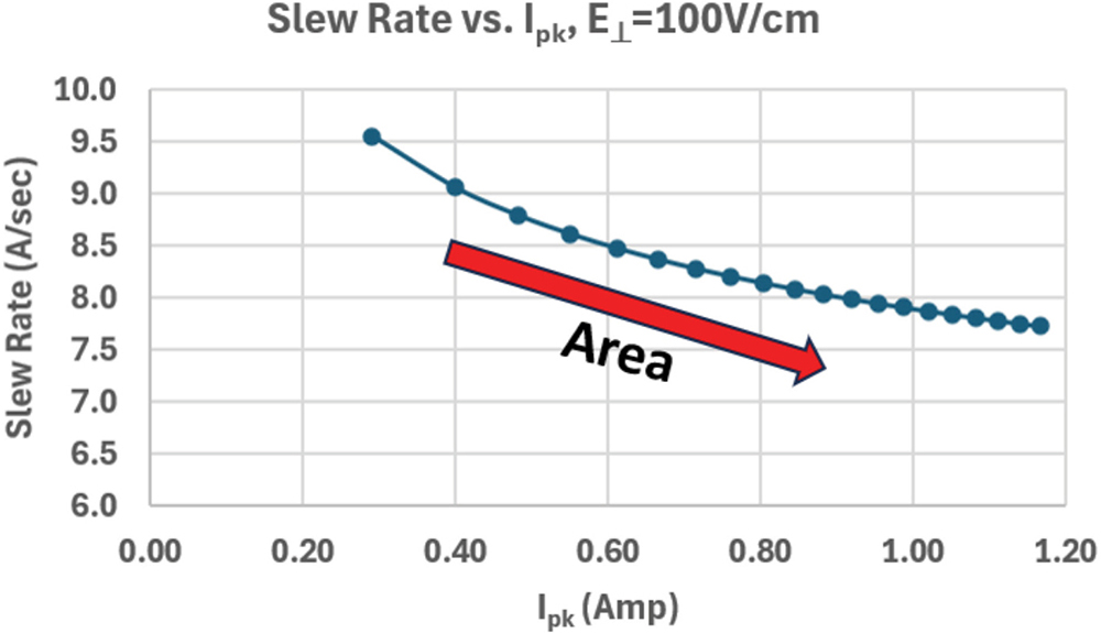
The same data for Ipk and slew rate are plotted in Figure 6, showing a boundary in the Ipk-slew rate plane beyond which (above and to the right) one would want to achieve passing CDM test results, in order to assure robustness beyond the limits. As E varies, the scales shrink by the same factor. Conversely, one could think of a passing test result beyond the boundary as “clearing” the component to a higher E value, one for Ipk and one for slew rate. We expect that for a given E, we will have to use a higher Ipk value to achieve the desired slew rate, therefore, the E goals for Ipk can be higher than for slew rate.
Figure 6: Maximum slew rate-peak current boundary curve for E⊥= 100V/cm. A “good” device would be one that passes CDM testing above and to the right of the curve.
Figure 6: Maximum slew rate-peak current boundary curve for E= 100V/cm. A “good” device would be one that passes CDM testing above and to the right of the curve.
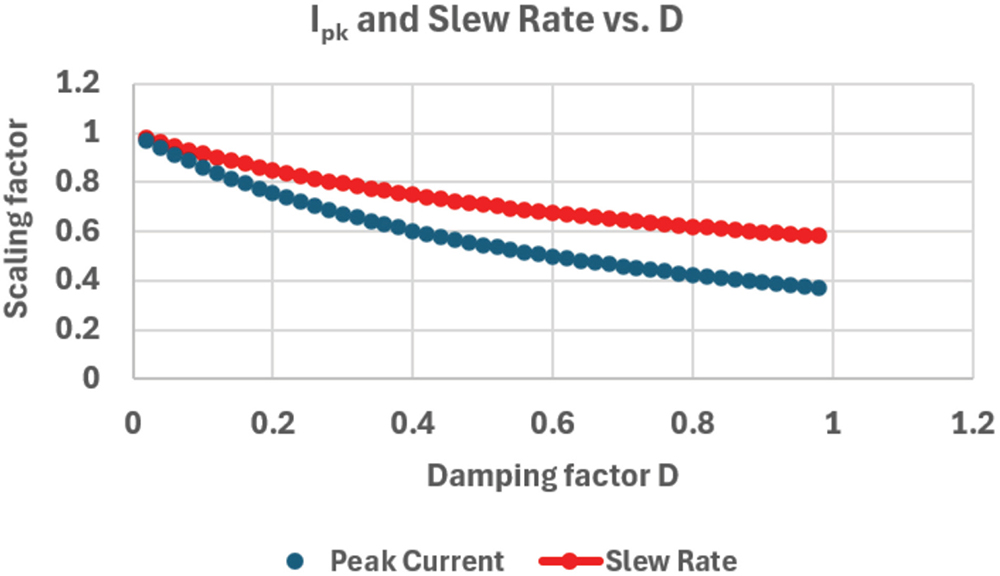
All CDM events are weakened by spark resistance, affecting the 2-pole damped sinusoid model through damping factor D, as seen in Equation 3 for Ipk, in the exponential factor. Once we are confident of a minimum D, worst-case Ipk degrades from the D=0 value (for any area A, as in Figure 3) as plotted in Figure 7.
Figure 7: Reduction of Ipk and slew rate worst case due to damping factor D = RCw0/2
Figure 7: Reduction of Ipk and slew rate worst case due to damping factor D = RCw0/2
Slew rate also degrades with D, although not as strongly, as also seen in Figure 7. For the slew rate vs. D, we use the Ipk value as reduced by D in Equation 3, then divide that by rise time tr, as derived from the general two pole solution in Reference 3, Appendix B, for the peak current time t0. We then take 2t0/π as the D-dependent rise time, in order to match up with D = 0 slew rate as in Equation 7 and reflecting the actual rise time. This is:
Equation 8
From a vast number of observed CDM waveforms, we find that the “cleanest” pulses, with low spark resistance, result in D no less than 0.25-0.3. Therefore, D = 0.2 would be a conservative value to use for reducing Ipk and slew rate goals. This means we could comfortably reduce Ipk to 75% of the D = 0 value and slew rate to 85% of the D = 0 value, even without recognizing that D is larger for larger area (and higher C) devices. The boundary curve of Figure 6 and CDM target goals for given E would be affected accordingly.

We now have a clearer idea of how waveform goals of Ipk and slew rate can match up with, say, the test condition goals of JS = 002 (see Reference 1). For example, TC125 in JS-002 asks for about 3A peak current and <350 ps rise time, i.e., about 9 A/nsec slew rate, for the large CDM target (about 5 cm2). Referring to Figures 3-6, a passing result for a 5 cm2 device to TC125 would mean clearance of E = 500V/cm for Ipk, but of just over 100V/cm if slew rate under test was barely passing. Even so, 100V/cm is considered a reasonable static control goal at present, and it could be reduced further in the future by using more aggressive static control, the kind long used in the manufacture of magnetic tape heads, when needed.

The reader is invited to apply these concepts to the 1 cm2 target discussed in Reference 2, II.B.2, surrounding Figures 8 and 9, and adapted from a 2024 study (see Reference 4). Numbers work out very well for rise time, slew rate, and Ipk limits, using D = 0.3, and if √LC is computed from the circuit modeled waveform values. Evidently, L is reduced by the 2 mm diameter pedestal for discharge, artificially suppressing some of the magnetic field that slows things down. The equivalent field from this tribocharged device (no static control applied, maximum tool speed) is 376V/cm.

Conclusion
In conclusion, we hope that the study discussed in this article helps prepare the design and test community for setting future CDM test goals for products that will be exposed to CDM events in manufacturing and use. We have tried to show how goals should center around peak current and slew rate, and how CDM testing can align those waveform properties with use conditions.
References
  1. ANSI/ESDA/JEDEC JS-002-2025, Charged Device Model (CDM)-Device Level test standard, July 2025.
  2. T.J. Maloney, “Radial Transmission Line Effects in Charged Device Model Events and Testing,” 2025 EOS/ESD Symposium, Riverside, CA, September 15-17, 2025, paper 4A.2.
  3. T. Maloney and N. Jack, “CDM Tester Properties as Deduced from Waveforms,” IEEE TDMR-14, pp. 792-800, 2014.
  4. E. Jirutkova, H. Wolf, H. Gieser, “In-situ ESD Current Sensing in a Pick and Place Machine,” 2024 EOS/ESD Symposium, Reno, NV, paper M1.1.

Share this story:
Timothy J. Malone
The Authors
Timothy J. Maloney is a Fellow of the IEEE and the co-author of the book, Basic ESD and I/O Design (Wiley, 1998). He spent much of his 40-plus-year career as a Senior Principal Engineer at Intel Corporation. Maloney can be reached at tjmaloney@sbcglobal.net.

Peyman Ensaf
Peyman Ensaf is a Principal Electromagnetic Effects Engineer at Boeing and can be reached at peyman.ensaf@boeing.com.