




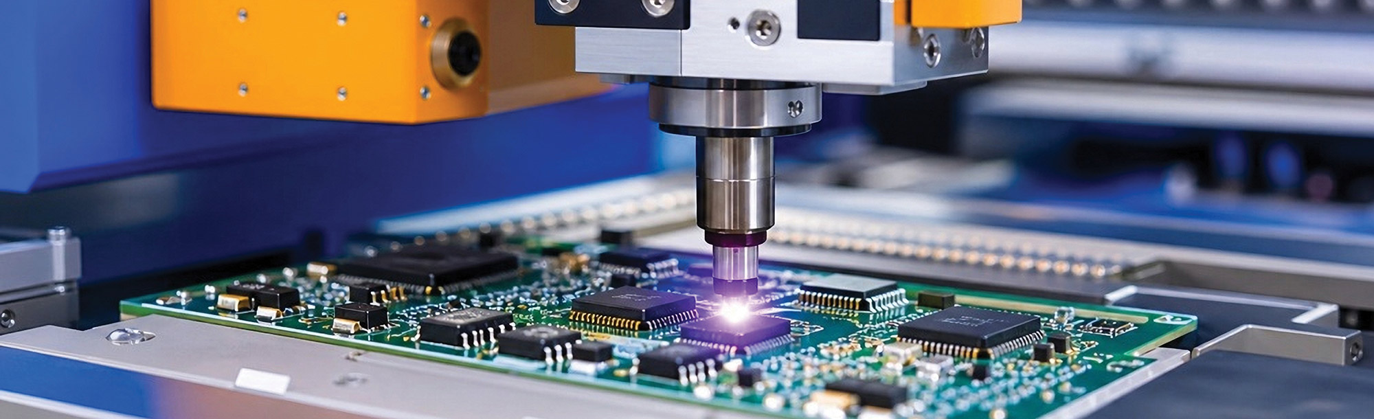
In-Situ ESD Current Sensing in a Pick and Place Machine



ISSN 1948-8254 (print)
ISSN 1948-8262 (online)
is published by
Same Page Publishing Inc.
451 King Street, #458
Littleton, MA 01460
tel: (978) 486-4684
fax: (978) 486-4691
© Copyright 2026 Same Page Publishing, Inc. all rights reserved
Contents may not be reproduced in any form without the prior consent of the publisher. While every attempt is made to provide accurate information, neither the publisher nor the authors accept any liability for errors or omissions.
editor-in-chief
Please contact our circulation department at circulation@incompliancemag.com







The FCC voted to approve a Report and Order, Order of Proposed Modification, and Order on Reconsideration authorizing the auction of 160 megahertz of spectrum in the upper C-band (3.98‑4.14 GHz). The order also adopts new rules intended to harmonize terrestrial wireless…

The press release from the Office of FCC Chair Brendan Carr details 30 specific changes to the agency’s rules, regulations, and procedures that will “unleash fast and affordable services for American families and businesses.”

Product Line Director
Spectrum Control, Inc.

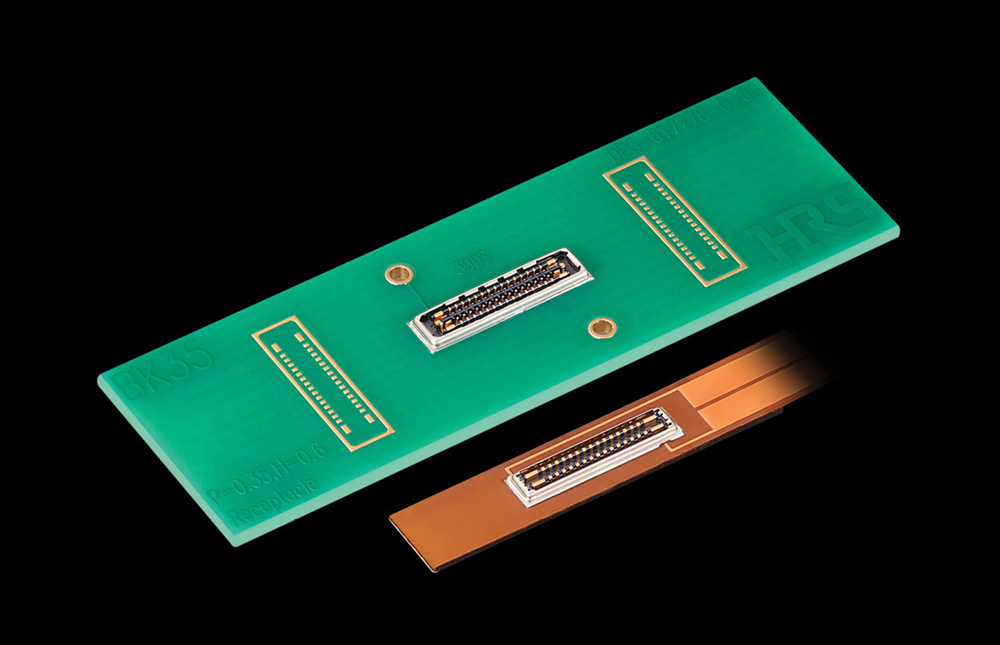
Electronic systems are becoming more integrated, combining high-speed digital communications, sensitive analog electronics, higher power densities, and increasingly compact packaging within the same design. At the same time, system architects face growing pressure to reduce size, weight, power, and cost (SWaP-C), leaving less room for discrete EMI mitigation added later in development. As more power and signal interfaces are incorporated into modern platforms, conducted interference can propagate throughout a system before it is identified during compliance testing, when corrective actions are often expensive and disruptive. These trends are changing the way engineers approach EMC, shifting the focus from treating compliance as a final test event to considering interference as a system-level design challenge from the very beginning.
Reducing EMC risk begins by evaluating every electrical interface as part of the overall system architecture rather than waiting until hardware integration is complete. Power entry points, external I/O, cable harnesses, and subsystem connections should all be assessed as potential pathways for conducted interference. Early planning allows engineers to develop an EMC strategy that combines grounding, shielding, filtering, and layout practices where they will have the greatest impact. As SWaP-C (Size, Weight, Power, and Cost) constraints become increasingly important, integrating EMI protection directly into boundary interfaces can reduce component count, eliminate additional packaging, and simplify assembly without compromising performance. Addressing interference before it propagates through the system improves design flexibility while supporting a more efficient path toward successful compliance.
Considering EMC at system boundaries enables engineers to address interference before it affects sensitive electronics, reducing the likelihood of costly redesigns during qualification. Integrating multiple electrical functions into a single boundary solution can also reduce assembly complexity, improve reliability by minimizing interconnections, and support increasingly demanding SWaP-C objectives. Rather than adding discrete filtering components later in development, engineers can incorporate EMI protection as part of the overall system architecture, preserving valuable space while reducing weight and simplifying manufacturing. As electronic systems continue to increase in complexity, this design philosophy supports faster development cycles, more predictable qualification outcomes, and products that are better prepared for future technology advancements and evolving EMC requirements.


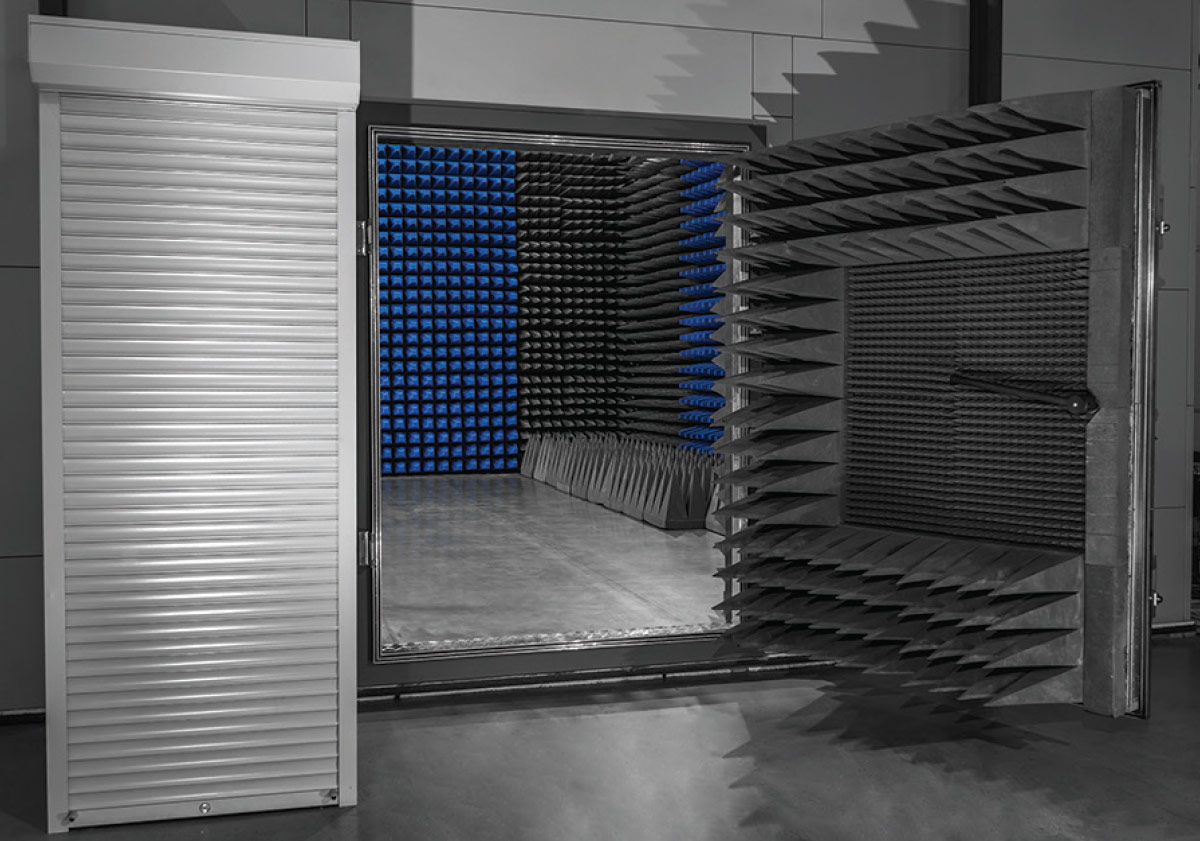
n the realm of electromagnetic compatibility (EMC), testing is crucial to ensure that electronic devices and systems operate without causing or being susceptible to electromagnetic interference (EMI). EMC test chambers provide controlled environments where comprehensive testing can be performed. These chambers are meticulously designed to block external electromagnetic fields and contain the emissions from the devices under test. This article explores the different types of EMC test chambers, key design considerations, and their applications across various industries.
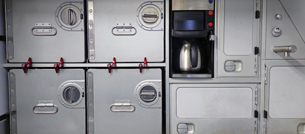
ne of the most critical aspects of aerospace EMI testing is that performed on the power lines of the equipment. The tests include various power line voltages, frequencies (for AC power), ramps, dropouts, surges, spikes, ripple, and the like. This paper will examine the characteristics of aircraft electrical power as specified in MIL-STD 704 and DO-160 Section 16.
First, about what is considered power. MIL-STD 704F, paragraph 6.10.1 states, “An aircraft electrical system is composed of a variety of power components (generation, conversion, inversion, control, power distribution, power management devices, etc.) that provide power to aircraft buses and utilization equipment terminals.”





t’s often said, by myself and many other EMC instructors, that good bonding is key for EMC success. And that’s true! But it leaves out some nuance: how good does “good” need to be?
It turns out that depends on what you need the bond to do for you. We usually talk in terms of preventing radio frequency interference (RFI), but there are several reasons you may need to pay close attention to your bonding scheme.
NASA-STD-4003A is a great document that packs a lot of practical information and guidance into a relatively short page count—less than 50, in the most recent version I have. It’s also publicly available for free! It defines bonding as: “The process of providing good electrical connection across faying surface mechanical interfaces to minimize electrical potential differences between equipment and individual parts of structure.” It then goes on to define five classes of bond…
n Part 2 of this series [1], we introduced you to radiated emissions pre-compliance testing for commercial, industrial, and medical products. Here, we’ll cover the differences in making the measurements for automotive modules and military products. In the next part of this series, we’ll describe some pre-compliance software that will help automate these manual measurements.
Readers will want to refer to the general test equipment setups, gain and loss calculations, and test procedures described in Parts 1 and 2. [1, 2] Additional details may be found in References 3 and 4.
Most automotive and military EMC tests for components, modules, or smaller products are tested in a similar environment to where the product is to be installed. This is a major difference in consumer testing in that we’re less concerned about interference to established communications and broadcast (TV, radio, aircraft, land mobile, and mobile phone) and more concerned with how a product behaves in the environment it’s designed for (automotive cockpits, military vehicles, shipboard, spacecraft, and military or commercial aircraft.

lectrostatic discharge (ESD) control programs often focus heavily on individual components, such as conductive flooring, ESD shoes, heel grounders, or wrist straps. Yet one of the most important lessons emerging from recent research is that no single component determines success. Instead, the interaction between footwear, flooring, environmental conditions, and human behavior ultimately dictates walking body voltage performance.
The ANSI/ESD S20.20 standard requires personnel grounding systems to maintain body voltages below 100 volts during normal movement. ANSI/ESD S20.20 also requires that the footwear/flooring system keeps body voltage below 100 volts when tested as a system per ANSI/ESD STM 97.2. While many facilities assume that installing an ESD floor or purchasing certified ESD footwear guarantees compliance, practical testing demonstrates that the reality is far more complex. Different combinations of floors and footwear can produce dramatically different results, even when each component independently satisfies specification requirements.



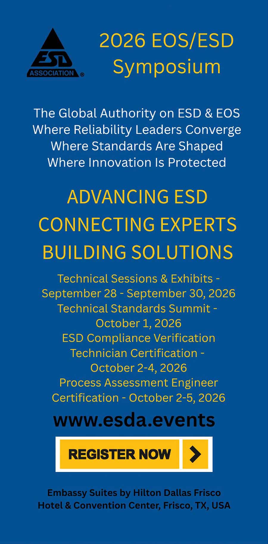
The event will feature an extensive lineup of keynotes, technical paper sessions, workshops, interactive seminars, and hands‑on training, covering the latest developments in AI and machine learning for ESD, advanced packaging and 3D integration, advanced node and high-voltage device design, test methods and standards, manufacturing and factory ESD control, system‑level ESD and high‑speed interfaces, harsh environment and radiation reliability, and electrostatics beyond semiconductors. These sessions are designed to equip you with cutting-edge knowledge that can be directly applied to your current and future projects.
Moreover, the symposium provides access to certification programs, enhancing your professional credentials, and a robust exhibit hall showcasing the latest tools and technologies. This is not just a chance to learn but also to connect with industry peers, share insights, and discuss challenges in an environment rich with networking opportunities.
In a field as specialized as ours, staying updated is not just beneficial, it’s essential. This symposium offers you the chance to refine your skills, expand your knowledge, and position yourself at the forefront of industry advancements.
We encourage you to attend to gain the expertise needed to excel in your role, and we hope to see you there!
Symposium & Exhibits



Frisco, Texas
- Engage in Cross-Disciplinary Learning
- Participate in Interactive Sessions
- Access Exclusive Content and Resources
- Stay updated on Regulatory Standards
- Explore Cutting Edge Technologies
- Expand your Professional Network
- AI and Machine Learning for ESD
- Advanced Packaging and 3D Integration
- Advanced Node and High-Voltage Device Design
- Test Methods and Standards
- Manufacturing and Factory ESD Control
- System-Level ESD and High-Speed Interfaces
- Harsh Environment and Radiation Reliability
- Electrostatics Beyond Semiconductors
Real-world lab data is expensive and slow to collect, and traditional supervised learning falls short when labeled data is scarce, particularly across multiple technology nodes where process variations shape ESD behavior differently. This session reviews machine learning techniques suited to limited or imbalanced datasets, then presents a scalable transfer learning framework combining a calibrated TCAD simulation model with a neural network classifier pre-trained on simulation data and fine-tuned on lab measurements. The approach correlates abnormalities to device physical variations, offering deeper insight into the design and process parameters influencing TLP variations.
Designing for harsh environments demands a shift in perspective: strong electrical latch-up performance is necessary but rarely sufficient. This talk bridges standard electrical reliability and the realities of radiation-induced failures, examining the space radiation environment, the effects of solar activity and orbital shielding on satellite electronics, and the particle cascade that creates terrestrial radiation events threatening aircraft and ground infrastructure. Comparing traditional latch-up with the more destructive Single Event Latch-up, it shows where standard design rules fall short and covers the mitigations and heavy-ion beam testing essential for extreme-environment hardware.
Demand for moving data continues to grow rapidly. The massive scale of modern large language models has led to an exponential increase in connectivity requirements within data centers, creating challenging scenarios for both training and inference. As users move closer, 5G networks are becoming saturated, with new deployments of massive MIMO needed to expand capacity without increasing costs or power consumption. This talk will explore these high-speed applications, with a particular focus on optical networking within data centers and radio units within base stations. New integrated circuit solutions will be discussed, with a focus on the challenges of protecting their interfaces as they move toward wider bandwidth and higher dynamic range.
Please see the EOS/ESD Symposium program for more information (https://www.esda.org).


hen we mention the charged device model (CDM) in electrostatic discharge (ESD), we could be referring to the essential factory event (referred to in this text as ChDE, or charged device event), or to the simulated event in a CDM tester, JS-002 in particular (see Reference 1).
A recent publication (Reference 2) used radial transmission line (RTL) theory to formulate the most accurate analytical model yet for these two versions of CDM, whereby a charged circular plate discharges at its center into a ground plate, as shown in Figure 1. RTL theory captures the essentials of both CDM cases and applies best to the real-world or actual use condition ChDE, again in Figure 1, representing component handling and die attach operations almost perfectly.
n the semiconductor industry, there is currently a growing trend towards Multi-Chip Modules (MCM) and Systems in a Package (SiP). These MCMs and SiPs consist of multiple dies/chiplets, sensors, and often delicate optoelectronic components that have minimal protection against Electrostatic Discharge (ESD). Figure 1 presents a schematic representation of such a MCM, including the internal pins, through silicon vias (TSV) and interposers, that do not have any connection to the outer world once assembled.


You can prepare for it.
Design. Testing. Compliance.
The expertise to address them shouldn’t be hard to find.

Always free for qualified professionals.
 https://incompliancemag.com
 info@incompliancemag.com
 In Compliance Magazine



October 13-16
Advanced PCB Design EMC+SI
Mechanical Design for EMC
October 26-29
You can do that here.