

his is Part 3 of our discussion on filter design for switched-mode power supplies. Previously, we discussed the basic operation of switched-mode power supplies, the role of the input and output capacitors, and the grounding design of isolated switched-mode power supplies.
In this article, we will demonstrate EMI filter design principles, especially the use of simulation tools such as SPICE software to accelerate the filter design process. Since a detailed SPICE model discussion is beyond the scope of this article, the focus here is instead on demonstrating the general concept of using SPICE‑based simulation tools during the EMI filter design process.
The simplest form of a low-pass filter can be an L-C filter. Therefore, the design engineer’s task is to choose an appropriate combination of inductance and capacitance values.
The design principle is to design the cut-off frequency of the filter to be well below the switching frequency (one-tenth as a rule of thumb). Therefore, in the case of a converter operating at a switching frequency of 400 kHz, would a low-pass filter with a cut-off frequency of 40 kHz be sufficient?
Figure 1 demonstrates this concept using a three-phase converter example. If we examine the output stage, we can observe a two-stage filter structure. The first stage typically consists of relatively large inductance and capacitance values, and its cut-off frequency is indeed designed around one tenth of the switching frequency. However, the second-stage filter is designed very differently from the first-stage filter. Therefore, it is important to clearly understand the roles and functions of these two different filters.
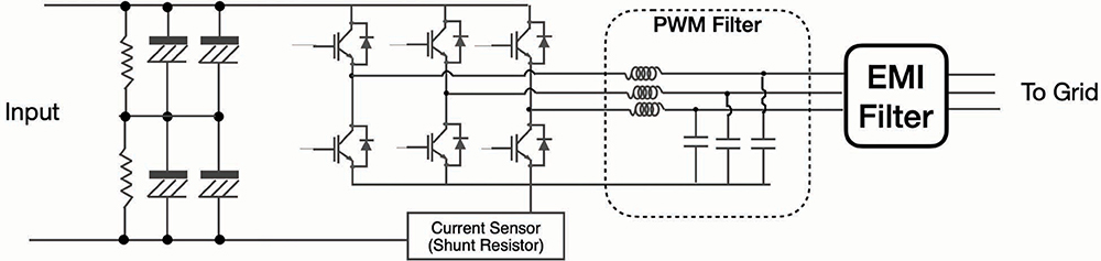
The second-stage filter is the EMI filter. Its purpose is to ensure that the conducted or radiated EMI noise is sufficiently low enough to achieve compliance requirements. Consequently, the design approach is more complicated than simply selecting a cut-off frequency.
To be clear, this article does not discuss the design of PWM filters, which is a completely different subject. PWM filter design requires the engineer to focus much more on ripple current, ripple voltage, thermal performance, physical size, and cost.
Since the purpose of the EMI filter is to achieve EMC compliance — or to achieve acceptable electromagnetic performance without causing EMI issues in real products — the first step is typically to understand the source and load impedance conditions. As demonstrated in Part 1 of our article series (see In Compliance Magazine, September 2025), the performance of any filter cannot be fully understood without considering the source-load impedance model.
But this raises an important question: is the source-load model actually well-defined in switched-mode power supplies?
The output impedance of a DC-DC converter is relatively straightforward to understand, since it is generally designed to be low impedance across a wide frequency range. Typically, the differential mode output impedance is reduced through the use of large amounts of output capacitance, although the PWM filter inductance also plays an important role in reducing ripple current within the converter.
The common mode impedance — that is, the relationship between the noise source and the test ground plane (chassis) — is much harder to define. It depends heavily on the output grounding strategy. For example, is the 5 V output return isolated from chassis ground, resulting primarily in capacitive coupling to ground? Or is it directly bonded to the chassis using a grounding strap, resulting in a more inductive coupling mechanism? At frequencies in the tens of MHz range, the common mode impedance arguably becomes relatively low due to capacitive coupling effects.
However, in this particular case, the filter design is not strongly influenced by the output impedance. Although the output impedance — and particularly the load impedance of the converter — does affect the common mode behavior, this topic will be discussed in a later article.
For the filter design discussed here, the input impedance of the converter is much more important. Unfortunately, the input impedance depends on many factors, including the input capacitor configuration, switching frequency, and feedback control loop design. As a result, the input impedance is rarely straightforward to calculate.
In many cases, negative impedance behavior is actually expected. Considering a constant power system, if the input voltage increases, the input current must decrease in order to maintain constant power. Therefore, this results in an effective negative impedance characteristic.
And this discussion only concerns the differential mode impedance. On the common mode side, similar to the earlier discussion on output impedance, the impedance again depends heavily on how the DUT is grounded. Cable length also plays an important role in determining high-frequency behavior, since electrically long cables can introduce resonances within the system.
Reference 2 demonstrates the measured input impedance of a small DC-DC converter under different input voltage conditions (shown in Figure 4). As the input voltage changes, the input impedance also changes significantly. It can be observed that the impedance may vary from tens of ohms to several hundreds of ohms depending on the operating condition.
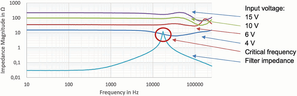
The key point readers should take away is that, for an EMI filter to operate effectively, the source-load impedance model used for differential mode analysis should realistically be considered as a varying source impedance driving a 100 Ω load impedance. For common mode analysis, the model should similarly be considered as a varying impedance driving a 25 Ω load impedance.
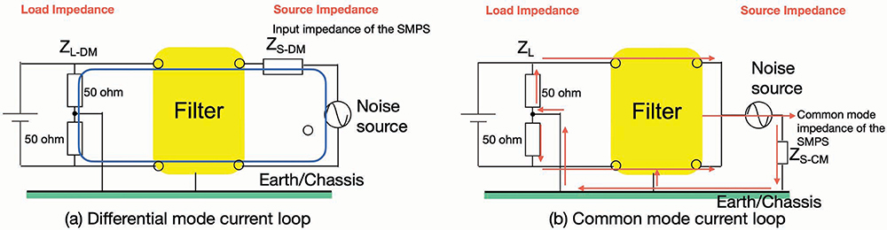
In reality, the system is almost never a simple 50 Ω/50 Ω environment, despite the fact that the majority of EMI filter manufacturers use 50 Ω/50 Ω insertion loss measurements to demonstrate filter performance.
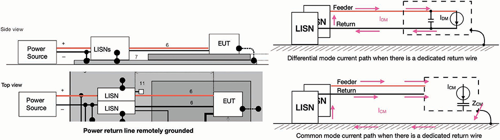
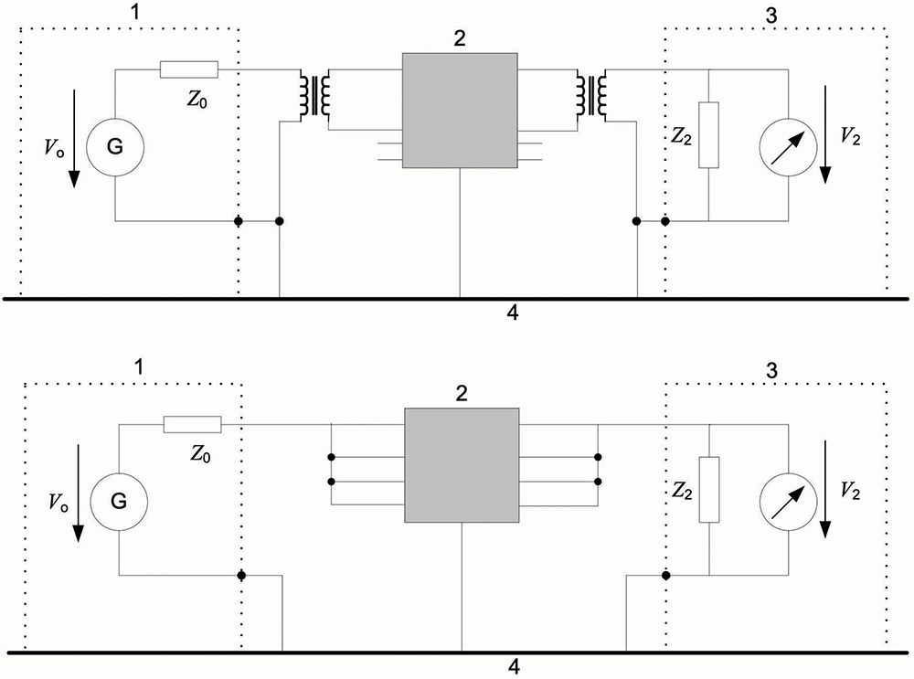
CISPR 17 defines two standard test methods for measuring filter performance: the symmetrical mode test (differential mode) and the asymmetrical mode test (common mode). The corresponding test setups are shown in Figure 5.
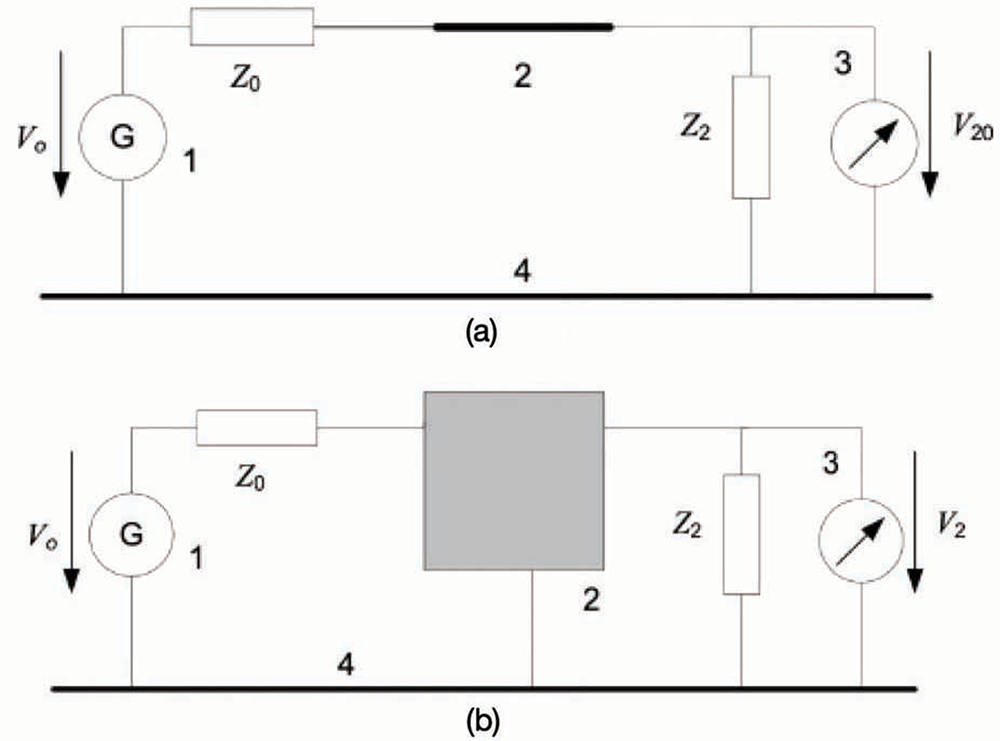
The insertion loss is defined as:
Insertion Loss = 20log(V20/v2)
- Where V20 is the voltage across Z2 before the filter is inserted, and
- V2 is the voltage measurement after the filter is inserted, as per Figure 6.
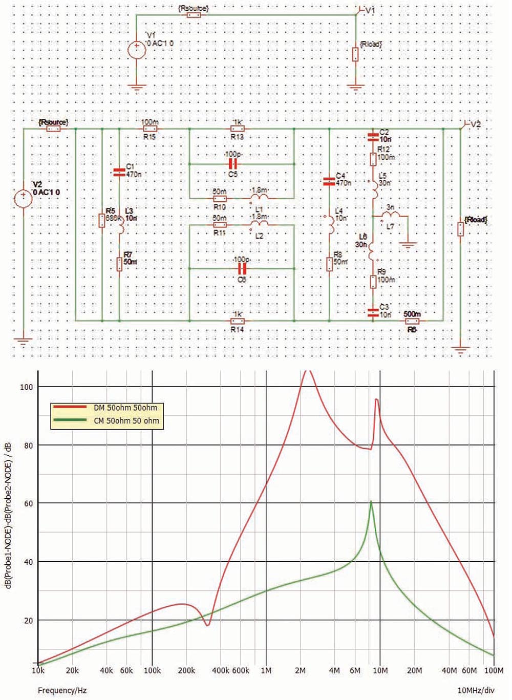
In this example, a filter containing both differential mode and common mode filtering elements was constructed. Note that the differential mode filtering inductance was obtained from the leakage inductance of the common mode choke. Within the simulation model, this behavior can be represented by assigning a coupling factor between L1 and L2 of less than one.
The parasitics associated with the inductive components include winding capacitance and damping effects introduced by the magnetic core material. For the capacitors, the parasitic elements mainly consist of equivalent series inductance (ESL) and equivalent series resistance (ESR), which engineers can typically obtain directly from the component manufacturer’s datasheets. We also included the trace and trace inductance when making the connections between the filter and the circuit.
The source and load impedances are implemented in the simulation model using purely resistive components, allowing the impedance values to be easily adjusted in order to simulate different source‑load configurations.
To begin with, the insertion loss was evaluated using a conventional 50 Ω/50 Ω source-load configuration, and both differential mode and common mode attenuation characteristics were obtained.
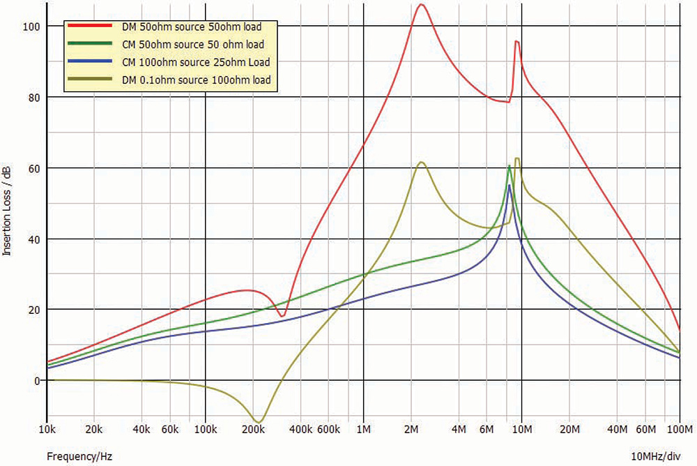
The simulation results show significant differences compared with the conventional 50 Ω/50 Ω source-load model. In this particular case, it can be observed that around 200 kHz, there is actually an insertion gain rather than an insertion loss. In other words, the noise at approximately 200 kHz is not attenuated by the filter but instead increases by more than 10 dB.
This is clearly a significant concern for conducted emissions performance. In some cases, such behavior may also contribute to control loop instability and other unexpected converter interactions. Therefore, identifying these effects early in the design stage is extremely important in order to avoid major surprises later during EMC compliance testing.
- Ken Javor, “Line Impedance Stabilization is in its Seventieth Year and Still Going Strong,” In Compliance Magazine, June 2023.
- Omicron Lab, “Input Impedance Measurements for Stable Input-Filter Design,” Application Note.
- International Electrotechnical Commission(IEC), CISPR 17, Methods of measurement of the suppression characteristics of passive EMC filtering devices, Edition 2.0 2011-06.

Dr. Min Zhang is a Senior Contributor to In Compliance Magazine, and the founder and principal EMC consultant of Mach One Design Ltd. (https://www.mach1design.co.uk), a UK-based engineering firm that specializes in EMC consulting, troubleshooting, and training. His in-depth knowledge of power electronics, digital electronics, electric machines, and product design has benefitted companies worldwide. Zhang can be reached at info@mach1design.co.uk